

111
Metal-Oxide-Semiconductor System
Equation 3.76 is an implicit relation in f s and must be solved numerically.
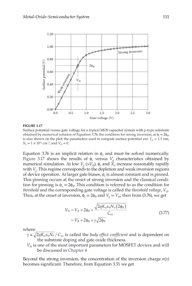
Figure 3.17 shows the results of f s versus V g characteristics obtained by
numerical simulation. At low V g (>V fb ), f s and X d increase reasonably rapidly
with V g . This regime corresponds to the depletion and weak inversion regions
of device operation. At larger gate biases, f s is almost constant and is pinned.
This pinning occurs at the onset of strong inversion and the classical condition for pinning is f s = 2f B . This condition is referred to as the condition for
threshold and the corresponding gate voltage is called the threshold voltage, V th .
Thus, at the onset of inversion, f s = 2f B and V g = V th ; then from (3.76), we get
V V
qK N
C
V
th
fb
B
si
a
B
ox
fb
B
B
=
+
+
( )
=
+
+
2
2
2
2
2
0
φ
ε
φ
φ γ φ
(3.77)
where:
γ
ε
≡ 2
0
qK N C
si
ox
a /
is called the body effect coefficient and is dependent on
the substrate doping and gate oxide thickness.
V th is one of the most important parameters for MOSFET devices and will
be discussed in Chapter 4
Beyond the strong inversion, the concentration of the inversion charge n(x)
becomes significant. Therefore, from Equation 3.51 we get
0.0
0.00
0.20
V th
2ϕ B
0.40
0.60
W e a k i n v e r s i o n
0.80
Stron g inver sion
1.00
1.20
0.5
1.0
1.5
Gate voltage (V)
Surface potential (V)
2.0
2.5
3.0
FIGURE 3.17
Surface potential versus gate voltage for a typical MOS capacitor system with p-type substrate
obtained by numerical solution of Equation 3.76; the condition for strong inversion, at f s = 2f B ,
is also shown on the plot; the parameters used to compute surface potential are: T ox = 1.5 nm,
N a = 1 × 10 16 cm –3 , and V fb = 0.
Metal-Oxide-Semiconductor System
Equation 3.76 is an implicit relation in f s and must be solved numerically.
Figure 3.17 shows the results of f s versus V g characteristics obtained by
numerical simulation. At low V g (>V fb ), f s and X d increase reasonably rapidly
with V g . This regime corresponds to the depletion and weak inversion regions
of device operation. At larger gate biases, f s is almost constant and is pinned.
This pinning occurs at the onset of strong inversion and the classical condition for pinning is f s = 2f B . This condition is referred to as the condition for
threshold and the corresponding gate voltage is called the threshold voltage, V th .
Thus, at the onset of inversion, f s = 2f B and V g = V th ; then from (3.76), we get
V V
qK N
C
V
th
fb
B
si
a
B
ox
fb
B
B
=
+
+
( )
=
+
+
2
2
2
2
2
0
φ
ε
φ
φ γ φ
(3.77)
where:
γ
ε
≡ 2
0
qK N C
si
ox
a /
is called the body effect coefficient and is dependent on
the substrate doping and gate oxide thickness.
V th is one of the most important parameters for MOSFET devices and will
be discussed in Chapter 4
Beyond the strong inversion, the concentration of the inversion charge n(x)
becomes significant. Therefore, from Equation 3.51 we get
0.0
0.00
0.20
V th
2ϕ B
0.40
0.60
W e a k i n v e r s i o n
0.80
Stron g inver sion
1.00
1.20
0.5
1.0
1.5
Gate voltage (V)
Surface potential (V)
2.0
2.5
3.0
FIGURE 3.17
Surface potential versus gate voltage for a typical MOS capacitor system with p-type substrate
obtained by numerical solution of Equation 3.76; the condition for strong inversion, at f s = 2f B ,
is also shown on the plot; the parameters used to compute surface potential are: T ox = 1.5 nm,
N a = 1 × 10 16 cm –3 , and V fb = 0.