

113
Metal-Oxide-Semiconductor System
It is also observed from Equation 3.79 that at the onset of strong inversion defined by f s = 2f B , the inversion layer concentration at the surface becomes equal
to the majority carrier concentration in the surface, that is, n(0) = N b .
Generally, inversion carriers must be treated quantum-mechanically as a
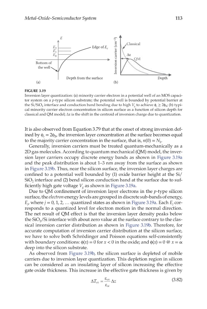
2D gas molecules. According to quantum mechanical (QM) model, the inversion layer carriers occupy discrete energy bands as shown in Figure 3.19a
and the peak distribution is about 1–3 nm away from the surface as shown
in Figure 3.19b. Thus, near the silicon surface, the inversion layer charges are
confined to a potential well bounded by (1) oxide barrier height at the Si/
SiO 2 interface and (2) bend silicon conduction band at the surface due to sufficiently high gate voltage V g as shown in Figure 3.19a.
Due to QM confinement of inversion layer electrons in the p-type silicon
surface, the electron energy levels are grouped in discrete sub-bands of energy,
E j , where j = 0, 1, 2, … quantized states as shown in Figure 3.19a. Each E j corresponds to a quantized level for electron motion in the normal direction.
The net result of QM effect is that the inversion layer density peaks below
the SiO 2 /Si interface with about zero value at the surface contrary to the classical inversion carrier distribution as shown in Figure 3.19b. Therefore, for
accurate computation of inversion carrier distribution at the silicon surface,
we have to solve both Schrödinger and Poisson equations self-consistently
with boundary conditions: f(x) = 0 for x < 0 in the oxide; and f(x) = 0 @ x = ∝
deep into the silicon substrate.
As observed from Figure 3.19b, the silicon surface is depleted of mobile
carriers due to inversion layer quantization. This depletion region in silicon
can be considered as an insulating layer of silicon increasing the effective
gate oxide thickness. This increase in the effective gate thickness is given by
∆
∆
T
z
ox
ox
si
=
ε
ε
(3.82)
Bottom of
the well
Edge of E c
E 2
E
E 1
E 0
Depth from the surface
(a)
(b)
Inversion carrier (cm −3
)
Depth
QM
Classical
Δz
FIGURE 3.19
Inversion layer quantization: (a) minority carrier electron in a potential well of an MOS capacitor system on a p-type silicon substrate; the potential well is bounded by potential barrier at
the Si/SiO 2 interface and conduction band bending due to high V g to achieve f s ≥ 2f B ; (b) typical minority carrier electron concentration in silicon surface as a function of silicon depth for
classical and QM model; Δz is the shift in the centroid of inversion charge due to quantization.
Metal-Oxide-Semiconductor System
It is also observed from Equation 3.79 that at the onset of strong inversion defined by f s = 2f B , the inversion layer concentration at the surface becomes equal
to the majority carrier concentration in the surface, that is, n(0) = N b .
Generally, inversion carriers must be treated quantum-mechanically as a
2D gas molecules. According to quantum mechanical (QM) model, the inversion layer carriers occupy discrete energy bands as shown in Figure 3.19a
and the peak distribution is about 1–3 nm away from the surface as shown
in Figure 3.19b. Thus, near the silicon surface, the inversion layer charges are
confined to a potential well bounded by (1) oxide barrier height at the Si/
SiO 2 interface and (2) bend silicon conduction band at the surface due to sufficiently high gate voltage V g as shown in Figure 3.19a.
Due to QM confinement of inversion layer electrons in the p-type silicon
surface, the electron energy levels are grouped in discrete sub-bands of energy,
E j , where j = 0, 1, 2, … quantized states as shown in Figure 3.19a. Each E j corresponds to a quantized level for electron motion in the normal direction.
The net result of QM effect is that the inversion layer density peaks below
the SiO 2 /Si interface with about zero value at the surface contrary to the classical inversion carrier distribution as shown in Figure 3.19b. Therefore, for
accurate computation of inversion carrier distribution at the silicon surface,
we have to solve both Schrödinger and Poisson equations self-consistently
with boundary conditions: f(x) = 0 for x < 0 in the oxide; and f(x) = 0 @ x = ∝
deep into the silicon substrate.
As observed from Figure 3.19b, the silicon surface is depleted of mobile
carriers due to inversion layer quantization. This depletion region in silicon
can be considered as an insulating layer of silicon increasing the effective
gate oxide thickness. This increase in the effective gate thickness is given by
∆
∆
T
z
ox
ox
si
=
ε
ε
(3.82)
Bottom of
the well
Edge of E c
E 2
E
E 1
E 0
Depth from the surface
(a)
(b)
Inversion carrier (cm −3
)
Depth
QM
Classical
Δz
FIGURE 3.19
Inversion layer quantization: (a) minority carrier electron in a potential well of an MOS capacitor system on a p-type silicon substrate; the potential well is bounded by potential barrier at
the Si/SiO 2 interface and conduction band bending due to high V g to achieve f s ≥ 2f B ; (b) typical minority carrier electron concentration in silicon surface as a function of silicon depth for
classical and QM model; Δz is the shift in the centroid of inversion charge due to quantization.