

105
Metal-Oxide-Semiconductor System
Q
v
s
s
kT
≈
−
(
)
exp
φ
2
accumulation
(3.55)
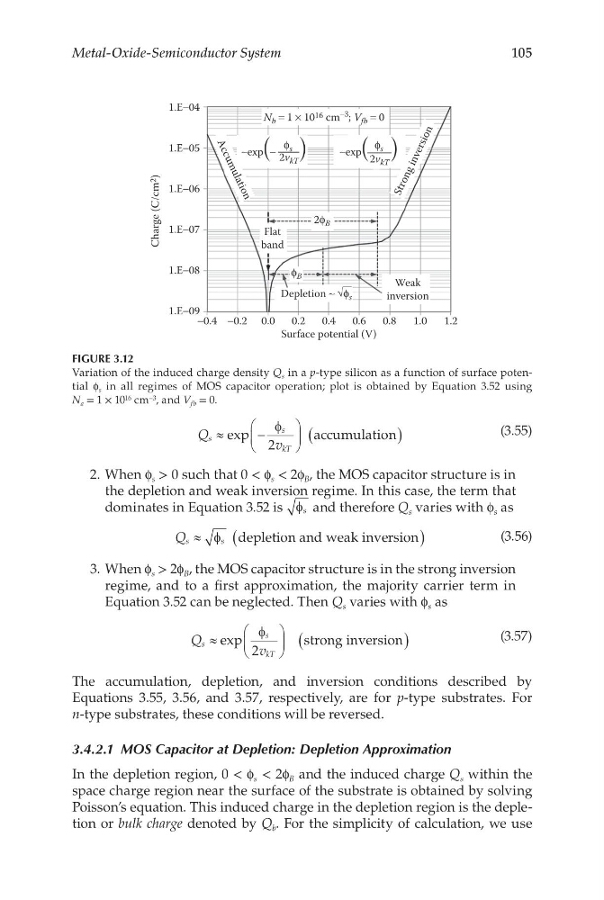
2. When f s > 0 such that 0 < f s < 2f B , the MOS capacitor structure is in
the depletion and weak inversion regime. In this case, the term that
dominates in Equation 3.52 is f s and therefore Q s varies with f s as
Q s
s
≈
(
)
φ depletion and weak inversion
(3.56)
3. When f s > 2f B , the MOS capacitor structure is in the strong inversion
regime, and to a first approximation, the majority carrier term in
Equation 3.52 can be neglected. Then Q s varies with f s as
Q
v
s
s
kT
≈
(
)
exp
φ
2
strong inversion
(3.57)
The accumulation, depletion, and inversion conditions described by
Equations 3.55, 3.56, and 3.57, respectively, are for p-type substrates. For
n-type substrates, these conditions will be reversed.
3.4.2.1 MOS Capacitor at Depletion: Depletion Approximation
In the depletion region, 0 < f s < 2f B and the induced charge Q s within the
space charge region near the surface of the substrate is obtained by solving
Poisson’s equation. This induced charge in the depletion region is the depletion or bulk charge denoted by Q b . For the simplicity of calculation, we use
−0.4
1.E−09
1.E−08
1.E−07
Charge (C/cm 2
)
1.E−06
1.E−05
1.E−04
A c c u m u la t io n
S t r o n g in v e r s io n
N b = 1 × 10 16 cm −3 ; V fb = 0
−0.2 0.0
Flat
band
0.2
0.4
Surface potential (V)
0.6
0.8
1.0
Weak
inversion
Depletion ∼ √ϕ s
1.2
2ϕ B
ϕ B
∼exp
ϕ s
2v kT
∼exp −
ϕ s
2v kT
FIGURE 3.12
Variation of the induced charge density Q s in a p-type silicon as a function of surface potential f s in all regimes of MOS capacitor operation; plot is obtained by Equation 3.52 using
N a = 1 × 10 16 cm –3 , and V fb = 0.
Metal-Oxide-Semiconductor System
Q
v
s
s
kT
≈
−
(
)
exp
φ
2
accumulation
(3.55)
2. When f s > 0 such that 0 < f s < 2f B , the MOS capacitor structure is in
the depletion and weak inversion regime. In this case, the term that
dominates in Equation 3.52 is f s and therefore Q s varies with f s as
Q s
s
≈
(
)
φ depletion and weak inversion
(3.56)
3. When f s > 2f B , the MOS capacitor structure is in the strong inversion
regime, and to a first approximation, the majority carrier term in
Equation 3.52 can be neglected. Then Q s varies with f s as
Q
v
s
s
kT
≈
(
)
exp
φ
2
strong inversion
(3.57)
The accumulation, depletion, and inversion conditions described by
Equations 3.55, 3.56, and 3.57, respectively, are for p-type substrates. For
n-type substrates, these conditions will be reversed.
3.4.2.1 MOS Capacitor at Depletion: Depletion Approximation
In the depletion region, 0 < f s < 2f B and the induced charge Q s within the
space charge region near the surface of the substrate is obtained by solving
Poisson’s equation. This induced charge in the depletion region is the depletion or bulk charge denoted by Q b . For the simplicity of calculation, we use
−0.4
1.E−09
1.E−08
1.E−07
Charge (C/cm 2
)
1.E−06
1.E−05
1.E−04
A c c u m u la t io n
S t r o n g in v e r s io n
N b = 1 × 10 16 cm −3 ; V fb = 0
−0.2 0.0
Flat
band
0.2
0.4
Surface potential (V)
0.6
0.8
1.0
Weak
inversion
Depletion ∼ √ϕ s
1.2
2ϕ B
ϕ B
∼exp
ϕ s
2v kT
∼exp −
ϕ s
2v kT
FIGURE 3.12
Variation of the induced charge density Q s in a p-type silicon as a function of surface potential f s in all regimes of MOS capacitor operation; plot is obtained by Equation 3.52 using
N a = 1 × 10 16 cm –3 , and V fb = 0.