

104
Compact Models for Integrated Circuit Design
d x
dx
qN v
K
e
x
v
n
a kT
si
x v
kT
kT
φ
ε
φ
φ
( )
( )
( )
=
+
−
+
−
2
0
2
1
i i
a
x v
kT
s
N
e
x
v
E x
kT
2
2
2
1
φ
φ
( )
( )
( )
−
−
=
(3.51)
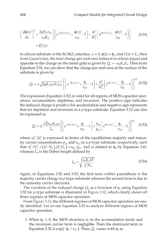
In silicon substrate at the Si/SiO 2 interface, x = 0, f(x) = f s , and E(x) = E s ; then
from Gauss’s law, the total charge per unit area induced in silicon (equal and
opposite to the charge on the metal gate) is given by Q
K E
s
s i s
= −ε 0
. Then from
Equation 3.51, we can show that the charge per unit area at the surface of the
substrate is given by
Q
q K N v
e
v
n
N
e
v
s
s i
a kT
v
s
kT
i
a
v
s
s kT
s kT
= ±
+
−
+
−
−(
)
(
)
2
1
0
2
2
ε
φ
φ
φ
φ
k kT
−
1
1 2
(3.52)
The expression (Equation 3.52) is valid for all regions of MOS capacitor operations: accumulation, depletion, and inversion. The positive sign indicates
the induced charge is positive for accumulation and negative sign represents
that for depletion and inversion in a p-type substrate. Equation 3.52 can also
be expressed as
Q
v K
L
e
v
n
p
e
v
s
kT si
d
v
s
kT
p
p
v
s
k
s kT
s kT
= ±
+
−
+
−
−(
)
(
)
2
1
0
ε
φ
φ
φ
φ
o
o
T T
−
1
1 2
(3.53)
where n N
i
a
2
2
is expressed in terms of the equilibrium majority and minority carrier concentrations p po and n po in a p-type substrate, respectively, such
that n N
n N
N
n p
i
a
i
a
a
p
p
2
2
2
1
= (
)( )=
.
o
o and is related to f B by Equation 3.41,
whereas L d is the Debye length defined by
L
K kT
q N
d
si
a
=
ε 0
2
(3.54)
Again, in Equations 3.52 and 3.53, the first term within parenthesis is the
majority carrier charge in p-type substrate whereas the second term is due to
the minority carrier electrons.
The variation of the induced charge Q s as a function of f s using Equation
3.52 for p-type substrate is illustrated in Figure 3.12, which clearly shows all
three regimes of MOS capacitor operation.
From Figure 3.12, the different regimes of MOS capacitor operation are easily identified. Let us use Equation 3.52 to analyze different regions of MOS
capacitor operation.
1. When f s < 0, the MOS structure is in the accumulation mode and
the inversion carrier term is negligible. Then the dominant term in
Equation 3.52 is exp
/
−
(
)
φ s k T
v . Thus, Q s varies with f s as
Compact Models for Integrated Circuit Design
d x
dx
qN v
K
e
x
v
n
a kT
si
x v
kT
kT
φ
ε
φ
φ
( )
( )
( )
=
+
−
+
−
2
0
2
1
i i
a
x v
kT
s
N
e
x
v
E x
kT
2
2
2
1
φ
φ
( )
( )
( )
−
−
=
(3.51)
In silicon substrate at the Si/SiO 2 interface, x = 0, f(x) = f s , and E(x) = E s ; then
from Gauss’s law, the total charge per unit area induced in silicon (equal and
opposite to the charge on the metal gate) is given by Q
K E
s
s i s
= −ε 0
. Then from
Equation 3.51, we can show that the charge per unit area at the surface of the
substrate is given by
Q
q K N v
e
v
n
N
e
v
s
s i
a kT
v
s
kT
i
a
v
s
s kT
s kT
= ±
+
−
+
−
−(
)
(
)
2
1
0
2
2
ε
φ
φ
φ
φ
k kT
−
1
1 2
(3.52)
The expression (Equation 3.52) is valid for all regions of MOS capacitor operations: accumulation, depletion, and inversion. The positive sign indicates
the induced charge is positive for accumulation and negative sign represents
that for depletion and inversion in a p-type substrate. Equation 3.52 can also
be expressed as
Q
v K
L
e
v
n
p
e
v
s
kT si
d
v
s
kT
p
p
v
s
k
s kT
s kT
= ±
+
−
+
−
−(
)
(
)
2
1
0
ε
φ
φ
φ
φ
o
o
T T
−
1
1 2
(3.53)
where n N
i
a
2
2
is expressed in terms of the equilibrium majority and minority carrier concentrations p po and n po in a p-type substrate, respectively, such
that n N
n N
N
n p
i
a
i
a
a
p
p
2
2
2
1
= (
)( )=
.
o
o and is related to f B by Equation 3.41,
whereas L d is the Debye length defined by
L
K kT
q N
d
si
a
=
ε 0
2
(3.54)
Again, in Equations 3.52 and 3.53, the first term within parenthesis is the
majority carrier charge in p-type substrate whereas the second term is due to
the minority carrier electrons.
The variation of the induced charge Q s as a function of f s using Equation
3.52 for p-type substrate is illustrated in Figure 3.12, which clearly shows all
three regimes of MOS capacitor operation.
From Figure 3.12, the different regimes of MOS capacitor operation are easily identified. Let us use Equation 3.52 to analyze different regions of MOS
capacitor operation.
1. When f s < 0, the MOS structure is in the accumulation mode and
the inversion carrier term is negligible. Then the dominant term in
Equation 3.52 is exp
/
−
(
)
φ s k T
v . Thus, Q s varies with f s as