

101
Metal-Oxide-Semiconductor System
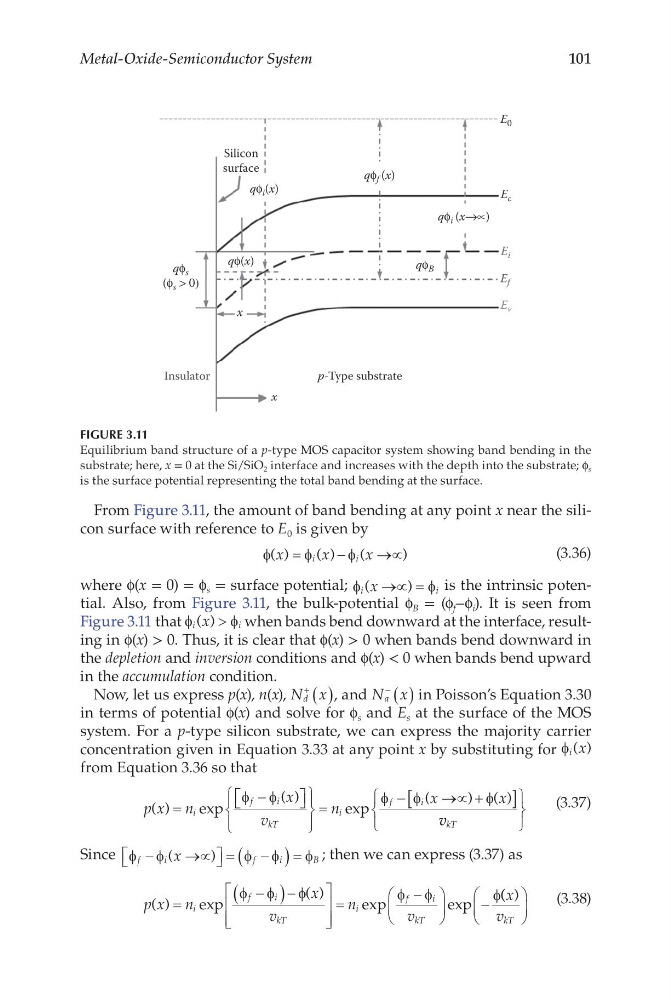
From Figure 3.11, the amount of band bending at any point x near the silicon surface with reference to E 0 is given by
φ
φ
φ
( )
( )
(
)
x
x
x
i
i
=
−
→∝
(3.36)
where f(x = 0) = f s = surface potential; φ
φ
i
i
x
(
)
→∝ = is the intrinsic potential. Also, from Figure 3.11, the bulk-potential f B = (f f –f i ). It is seen from
Figure 3.11 that φ
φ
i
i
x
( ) > when bands bend downward at the interface, resulting in f(x) > 0. Thus, it is clear that f(x) > 0 when bands bend downward in
the depletion and inversion conditions and f(x) < 0 when bands bend upward
in the accumulation condition.
Now, let us express p(x), n(x), N x
d
+
( ), and N x
a
−
( ) in Poisson’s Equation 3.30
in terms of potential f(x) and solve for f s and E s at the surface of the MOS
system. For a p-type silicon substrate, we can express the majority carrier
concentration given in Equation 3.33 at any point x by substituting for f i x
( )
from Equation 3.36 so that
p x n
x
v
n
x
x
i
f
i
kT
i
f
i
( )
exp
( )
exp
(
) ( )
=
−
=
−
→∝ +
[
]
φ φ
φ
φ
φ
v v kT
(3.37)
Since φ φ
φ φ
φ
f
i
f
i
B
x
−
→∝
=
−
(
) =
(
)
; then we can express (3.37) as
p x n
x
v
n
v
i
f
i
kT
i
f
i
kT
( )
exp
( )
exp
e xp
=
−
(
) −
=
−
−
φ φ
φ
φ φ
φ( ( )
x
v kT
(3.38)
Silicon
surface
x
x
Insulator
p-Type substrate
E 0
E c
E i
E f
E v
qϕ i (x)
qϕ s
(ϕ s > 0)
qϕ(x)
qϕ f (x)
qϕ B
qϕ i (x→∝)
FIGURE 3.11
Equilibrium band structure of a p-type MOS capacitor system showing band bending in the
substrate; here, x = 0 at the Si/SiO 2 interface and increases with the depth into the substrate; f s
is the surface potential representing the total band bending at the surface.
Metal-Oxide-Semiconductor System
From Figure 3.11, the amount of band bending at any point x near the silicon surface with reference to E 0 is given by
φ
φ
φ
( )
( )
(
)
x
x
x
i
i
=
−
→∝
(3.36)
where f(x = 0) = f s = surface potential; φ
φ
i
i
x
(
)
→∝ = is the intrinsic potential. Also, from Figure 3.11, the bulk-potential f B = (f f –f i ). It is seen from
Figure 3.11 that φ
φ
i
i
x
( ) > when bands bend downward at the interface, resulting in f(x) > 0. Thus, it is clear that f(x) > 0 when bands bend downward in
the depletion and inversion conditions and f(x) < 0 when bands bend upward
in the accumulation condition.
Now, let us express p(x), n(x), N x
d
+
( ), and N x
a
−
( ) in Poisson’s Equation 3.30
in terms of potential f(x) and solve for f s and E s at the surface of the MOS
system. For a p-type silicon substrate, we can express the majority carrier
concentration given in Equation 3.33 at any point x by substituting for f i x
( )
from Equation 3.36 so that
p x n
x
v
n
x
x
i
f
i
kT
i
f
i
( )
exp
( )
exp
(
) ( )
=
−
=
−
→∝ +
[
]
φ φ
φ
φ
φ
v v kT
(3.37)
Since φ φ
φ φ
φ
f
i
f
i
B
x
−
→∝
=
−
(
) =
(
)
; then we can express (3.37) as
p x n
x
v
n
v
i
f
i
kT
i
f
i
kT
( )
exp
( )
exp
e xp
=
−
(
) −
=
−
−
φ φ
φ
φ φ
φ( ( )
x
v kT
(3.38)
Silicon
surface
x
x
Insulator
p-Type substrate
E 0
E c
E i
E f
E v
qϕ i (x)
qϕ s
(ϕ s > 0)
qϕ(x)
qϕ f (x)
qϕ B
qϕ i (x→∝)
FIGURE 3.11
Equilibrium band structure of a p-type MOS capacitor system showing band bending in the
substrate; here, x = 0 at the Si/SiO 2 interface and increases with the depth into the substrate; f s
is the surface potential representing the total band bending at the surface.