

102
Compact Models for Integrated Circuit Design
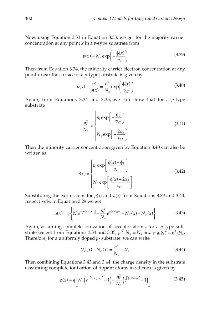
Now, using Equation 3.33 in Equation 3.38, we get for the majority carrier
concentration at any point x in a p-type substrate from
p x N
x
v
a
kT
( )
exp
( )
=
−
φ
(3.39)
Then from Equation 3.34, the minority carrier electron concentration at any
point x near the surface of a p-type substrate is given by
n x
n
p x
n
N
x
v
i
i
a
k T
( )
( )
exp
( )
≅
=
2
2
φ
(3.40)
Again, from Equations 3.34 and 3.35, we can show that for a p-type
substrate
n
N
n
v
N
v
i
a
i
B
kT
a
B
kT
2
2
=
−
−
exp
exp
φ
φ
(3.41)
Then the minority carrier concentration given by Equation 3.40 can also be
written as
n x
n
x
v
N
x
v
i
B
kT
a
B
kT
( )
exp
( )
exp
( )
=
−
−
φ
φ
φ
φ
2
(3.42)
Substituting the expressions for p(x) and n(x) from Equations 3.39 and 3.40,
respectively, in Equation 3.29 we get
ρ
φ
φ
( )
( )
( )
( )
( )
x q N e
n
N
e
N x N x
a
x v
i
a
x v
d
a
=
−
+
−
−
+
−
kT
kT
2
(3.43)
Again, assuming complete ionization of acceptor atoms, for a p-type substrate we get from Equations 3.34 and 3.35, p N
N
a
a
≅
≡
−
and n N
n N
d
i
a
≅
=
+
2
.
Therefore, for a uniformly doped p- substrate, we can write
N x N x
n
N
N
d
a
i
a
a
+
−
−
=
−
( )
( )
2
(3.44)
Then combining Equations 3.43 and 3.44, the charge density in the substrate
(assuming complete ionization of dopant atoms in silicon) is given by
ρ
φ
φ
( )
( )
( )
x q N e
n
N
e
a
x v
i
a
x v
kT
kT
=
−
(
) −
−
(
)
−
1
1
2
(3.45)
Compact Models for Integrated Circuit Design
Now, using Equation 3.33 in Equation 3.38, we get for the majority carrier
concentration at any point x in a p-type substrate from
p x N
x
v
a
kT
( )
exp
( )
=
−
φ
(3.39)
Then from Equation 3.34, the minority carrier electron concentration at any
point x near the surface of a p-type substrate is given by
n x
n
p x
n
N
x
v
i
i
a
k T
( )
( )
exp
( )
≅
=
2
2
φ
(3.40)
Again, from Equations 3.34 and 3.35, we can show that for a p-type
substrate
n
N
n
v
N
v
i
a
i
B
kT
a
B
kT
2
2
=
−
−
exp
exp
φ
φ
(3.41)
Then the minority carrier concentration given by Equation 3.40 can also be
written as
n x
n
x
v
N
x
v
i
B
kT
a
B
kT
( )
exp
( )
exp
( )
=
−
−
φ
φ
φ
φ
2
(3.42)
Substituting the expressions for p(x) and n(x) from Equations 3.39 and 3.40,
respectively, in Equation 3.29 we get
ρ
φ
φ
( )
( )
( )
( )
( )
x q N e
n
N
e
N x N x
a
x v
i
a
x v
d
a
=
−
+
−
−
+
−
kT
kT
2
(3.43)
Again, assuming complete ionization of acceptor atoms, for a p-type substrate we get from Equations 3.34 and 3.35, p N
N
a
a
≅
≡
−
and n N
n N
d
i
a
≅
=
+
2
.
Therefore, for a uniformly doped p- substrate, we can write
N x N x
n
N
N
d
a
i
a
a
+
−
−
=
−
( )
( )
2
(3.44)
Then combining Equations 3.43 and 3.44, the charge density in the substrate
(assuming complete ionization of dopant atoms in silicon) is given by
ρ
φ
φ
( )
( )
( )
x q N e
n
N
e
a
x v
i
a
x v
kT
kT
=
−
(
) −
−
(
)
−
1
1
2
(3.45)