

100
Compact Models for Integrated Circuit Design
3.4.1 Formulation of Poisson’s Equation in Terms
of Band-Bending Potential
In order to solve Poisson’s Equation 3.30 for f(x) at any point x near the surface
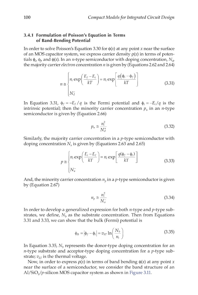
of an MOS capacitor system, we express carrier density ρ(x) in terms of potentials f i , f f , and f(x). In an n-type semiconductor with doping concentration, N d ,
the majority carrier electron concentration n is given by (Equations 2.62 and 2.64)
n
n
E E
kT
n
q
kT
N
i
f
i
i
i
f
d
≅
−
=
−
(
)
+
exp
e xp
φ φ
(3.31)
In Equation 3.31, φ f
f
E q
= − / is the Fermi potential and φ i
i
E q
= − / is the
intrinsic potential; then the minority carrier concentration p n in an n-type
semiconductor is given by (Equation 2.66)
p
n
N
n
i
d
≅ +
2
(3.32)
Similarly, the majority carrier concentration in a p-type semiconductor with
doping concentration N a is given by (Equations 2.63 and 2.65)
p
n
E E
kT
n
q
kT
N
i
i
f
i
f
i
a
≅
−
=
−
−
exp
e xp
(
)
φ φ
(3.33)
And, the minority carrier concentration n p in a p-type semiconductor is given
by (Equation 2.67)
n
n
N
p
i
a
≅ −
2
(3.34)
In order to develop a generalized expression for both n-type and p-type substrates, we define, N b as the substrate concentration. Then from Equations
3.31 and 3.33, we can show that the bulk (Fermi) potential is
φ
φ φ
B
f
i
k T
b
i
v
N
n
= − =
ln
(3.35)
In Equation 3.35, N b represents the donor-type doping concentration for an
n-type substrate and acceptor-type doping concentration for a p-type substrate; v kT is the thermal voltage.
Now, in order to express ρ(x) in terms of band bending f(x) at any point x
near the surface of a semiconductor, we consider the band structure of an
Al/SiO 2 /p-silicon MOS capacitor system as shown in Figure 3.11.
Compact Models for Integrated Circuit Design
3.4.1 Formulation of Poisson’s Equation in Terms
of Band-Bending Potential
In order to solve Poisson’s Equation 3.30 for f(x) at any point x near the surface
of an MOS capacitor system, we express carrier density ρ(x) in terms of potentials f i , f f , and f(x). In an n-type semiconductor with doping concentration, N d ,
the majority carrier electron concentration n is given by (Equations 2.62 and 2.64)
n
n
E E
kT
n
q
kT
N
i
f
i
i
i
f
d
≅
−
=
−
(
)
+
exp
e xp
φ φ
(3.31)
In Equation 3.31, φ f
f
E q
= − / is the Fermi potential and φ i
i
E q
= − / is the
intrinsic potential; then the minority carrier concentration p n in an n-type
semiconductor is given by (Equation 2.66)
p
n
N
n
i
d
≅ +
2
(3.32)
Similarly, the majority carrier concentration in a p-type semiconductor with
doping concentration N a is given by (Equations 2.63 and 2.65)
p
n
E E
kT
n
q
kT
N
i
i
f
i
f
i
a
≅
−
=
−
−
exp
e xp
(
)
φ φ
(3.33)
And, the minority carrier concentration n p in a p-type semiconductor is given
by (Equation 2.67)
n
n
N
p
i
a
≅ −
2
(3.34)
In order to develop a generalized expression for both n-type and p-type substrates, we define, N b as the substrate concentration. Then from Equations
3.31 and 3.33, we can show that the bulk (Fermi) potential is
φ
φ φ
B
f
i
k T
b
i
v
N
n
= − =
ln
(3.35)
In Equation 3.35, N b represents the donor-type doping concentration for an
n-type substrate and acceptor-type doping concentration for a p-type substrate; v kT is the thermal voltage.
Now, in order to express ρ(x) in terms of band bending f(x) at any point x
near the surface of a semiconductor, we consider the band structure of an
Al/SiO 2 /p-silicon MOS capacitor system as shown in Figure 3.11.