

99
Metal-Oxide-Semiconductor System
an MOS capacitor system originate from thermally generated electron–hole
pairs within the depletion region. The rate of thermal generation depends
upon the minority carrier lifetime, which is of the order of microseconds.
It is found that the time required to form an inversion layer at the surface
is about 0.2 sec [3]. Thus, the formation of the inversion layer is a relatively slow
process compared to the time required for the holes (majority carriers) to flow from or
to the silicon surface, which is of the order of picoseconds. Once the inversion
layer is formed, it shields the underneath depletion layer, thus limiting the
maximum width, X dmax , of the depletion layer.
So far, we have presented a qualitative overview of the basic operation of
an MOS capacitor system. In the following section, we will develop MOS
capacitor theory that can be extended to develop the operational theory of
MOSFET devices in Chapters 4, 5, and 9.
3.4 MOS Capacitor Theory
Now, let us derive the relation between the surface potential (f s ), electric
field (E s ), and charge (Q s ) by solving Poisson’s equation for potential (f) near
the surface region of the silicon substrate of an MOS capacitor system. The
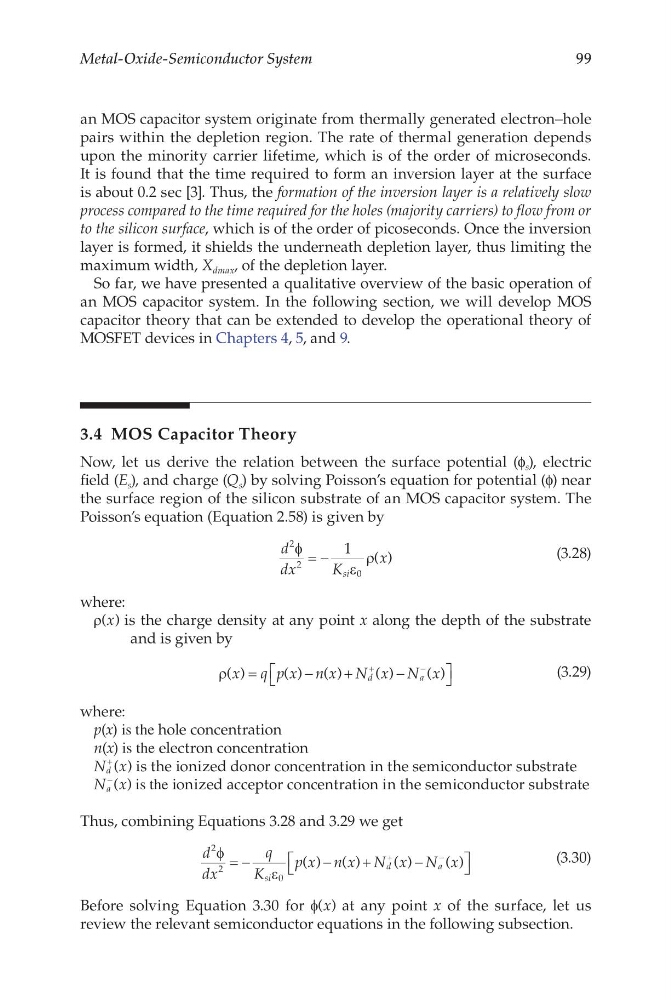
Poisson’s equation (Equation 2.58) is given by
d
dx
K
x
si
2
2
0
1
φ
ε
ρ
= −
( )
(3.28)
where:
ρ( )
x is the charge density at any point x along the depth of the substrate
and is given by
ρ( )
( ) ( )
( )
( )
x q p x n x N x N x
d
a
=
−
+
−
+
−
(3.29)
where:
p(x) is the hole concentration
n(x) is the electron concentration
N x
d
+ ( ) is the ionized donor concentration in the semiconductor substrate
N x
a
− ( ) is the ionized acceptor concentration in the semiconductor substrate
Thus, combining Equations 3.28 and 3.29 we get
d
dx
q
K
p x n x N x N x
si
d
a
2
2
0
φ
ε
= −
−
+
−
+
−
( ) ( )
( )
( )
(3.30)
Before solving Equation 3.30 for f( )
x at any point x of the surface, let us
review the relevant semiconductor equations in the following subsection.
Metal-Oxide-Semiconductor System
an MOS capacitor system originate from thermally generated electron–hole
pairs within the depletion region. The rate of thermal generation depends
upon the minority carrier lifetime, which is of the order of microseconds.
It is found that the time required to form an inversion layer at the surface
is about 0.2 sec [3]. Thus, the formation of the inversion layer is a relatively slow
process compared to the time required for the holes (majority carriers) to flow from or
to the silicon surface, which is of the order of picoseconds. Once the inversion
layer is formed, it shields the underneath depletion layer, thus limiting the
maximum width, X dmax , of the depletion layer.
So far, we have presented a qualitative overview of the basic operation of
an MOS capacitor system. In the following section, we will develop MOS
capacitor theory that can be extended to develop the operational theory of
MOSFET devices in Chapters 4, 5, and 9.
3.4 MOS Capacitor Theory
Now, let us derive the relation between the surface potential (f s ), electric
field (E s ), and charge (Q s ) by solving Poisson’s equation for potential (f) near
the surface region of the silicon substrate of an MOS capacitor system. The
Poisson’s equation (Equation 2.58) is given by
d
dx
K
x
si
2
2
0
1
φ
ε
ρ
= −
( )
(3.28)
where:
ρ( )
x is the charge density at any point x along the depth of the substrate
and is given by
ρ( )
( ) ( )
( )
( )
x q p x n x N x N x
d
a
=
−
+
−
+
−
(3.29)
where:
p(x) is the hole concentration
n(x) is the electron concentration
N x
d
+ ( ) is the ionized donor concentration in the semiconductor substrate
N x
a
− ( ) is the ionized acceptor concentration in the semiconductor substrate
Thus, combining Equations 3.28 and 3.29 we get
d
dx
q
K
p x n x N x N x
si
d
a
2
2
0
φ
ε
= −
−
+
−
+
−
( ) ( )
( )
( )
(3.30)
Before solving Equation 3.30 for f( )
x at any point x of the surface, let us
review the relevant semiconductor equations in the following subsection.