

98
Compact Models for Integrated Circuit Design
surface, that is, E f > E i . At this condition, the surface behaves like an n-type
material with an electron concentration given by (Equation 2.62)
n n
E E
kT
i
f
i
=
−
exp
(3.26)
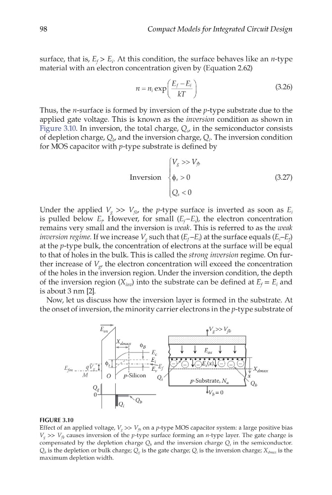
Thus, the n-surface is formed by inversion of the p-type substrate due to the
applied gate voltage. This is known as the inversion condition as shown in
Figure 3.10. In inversion, the total charge, Q s , in the semiconductor consists
of depletion charge, Q b , and the inversion charge, Q i . The inversion condition
for MOS capacitor with p-type substrate is defined by
Inversion
V
V
Q
g
f b
s
s
>>
>
<
φ 0
0
(3.27)
Under the applied V g >> V fb , the p-type surface is inverted as soon as E i
is pulled below E f . However, for small (E f –E i ), the electron concentration
remains very small and the inversion is weak. This is referred to as the weak
inversion regime. If we increase V g such that (E f –E i ) at the surface equals (E i –E f )
at the p-type bulk, the concentration of electrons at the surface will be equal
to that of holes in the bulk. This is called the strong inversion regime. On further increase of V g , the electron concentration will exceed the concentration
of the holes in the inversion region. Under the inversion condition, the depth
of the inversion region (X inv ) into the substrate can be defined at E f = E i and
is about 3 nm [2].
Now, let us discuss how the inversion layer is formed in the substrate. At
the onset of inversion, the minority carrier electrons in the p-type substrate of
Q b
Q i
Q g
0
E fm
M
qV g
E c
E f
E v
E i
E ox
X dmax
X dmax
ϕ B
ϕ s
p-Silicon
p-Substrate, N a
Q b
Q i
O
x
V b = 0
E ox
E s (x)
V g >> V fb
FIGURE 3.10
Effect of an applied voltage, V g >> V fb on a p-type MOS capacitor system: a large positive bias
V g >> V fb causes inversion of the p-type surface forming an n-type layer. The gate charge is
compensated by the depletion charge Q b and the inversion charge Q i in the semiconductor.
Q b is the depletion or bulk charge; Q g is the gate charge; Q i is the inversion charge; X dmax is the
maximum depletion width.
Compact Models for Integrated Circuit Design
surface, that is, E f > E i . At this condition, the surface behaves like an n-type
material with an electron concentration given by (Equation 2.62)
n n
E E
kT
i
f
i
=
−
exp
(3.26)
Thus, the n-surface is formed by inversion of the p-type substrate due to the
applied gate voltage. This is known as the inversion condition as shown in
Figure 3.10. In inversion, the total charge, Q s , in the semiconductor consists
of depletion charge, Q b , and the inversion charge, Q i . The inversion condition
for MOS capacitor with p-type substrate is defined by
Inversion
V
V
Q
g
f b
s
s
>>
>
<
φ 0
0
(3.27)
Under the applied V g >> V fb , the p-type surface is inverted as soon as E i
is pulled below E f . However, for small (E f –E i ), the electron concentration
remains very small and the inversion is weak. This is referred to as the weak
inversion regime. If we increase V g such that (E f –E i ) at the surface equals (E i –E f )
at the p-type bulk, the concentration of electrons at the surface will be equal
to that of holes in the bulk. This is called the strong inversion regime. On further increase of V g , the electron concentration will exceed the concentration
of the holes in the inversion region. Under the inversion condition, the depth
of the inversion region (X inv ) into the substrate can be defined at E f = E i and
is about 3 nm [2].
Now, let us discuss how the inversion layer is formed in the substrate. At
the onset of inversion, the minority carrier electrons in the p-type substrate of
Q b
Q i
Q g
0
E fm
M
qV g
E c
E f
E v
E i
E ox
X dmax
X dmax
ϕ B
ϕ s
p-Silicon
p-Substrate, N a
Q b
Q i
O
x
V b = 0
E ox
E s (x)
V g >> V fb
FIGURE 3.10
Effect of an applied voltage, V g >> V fb on a p-type MOS capacitor system: a large positive bias
V g >> V fb causes inversion of the p-type surface forming an n-type layer. The gate charge is
compensated by the depletion charge Q b and the inversion charge Q i in the semiconductor.
Q b is the depletion or bulk charge; Q g is the gate charge; Q i is the inversion charge; X dmax is the
maximum depletion width.