

97
Metal-Oxide-Semiconductor System
This bias condition (Equation 3.24) is useful in the characterization of MOS
capacitor system.
3.3.2 Depletion
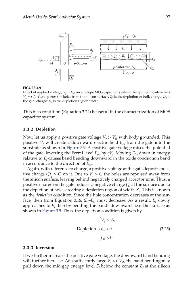
Now, let us apply a positive gate voltage V g > V fb with body grounded. This
positive V g will create a downward electric field E ox from the gate into the
substrate as shown in Figure 3.9. A positive gate voltage raises the potential
of the gate, lowering the Fermi level E fm by qV g . Moving E fm down in energy
relative to E f causes band bending downward in the oxide conduction band
in accordance to the direction of E ox .
Again, with reference to charge, a positive voltage at the gate deposits positive charge (Q g > 0) on it. Due to V g > 0, the holes are repulsed away from
the silicon surface, leaving behind negatively charged acceptor ions. Thus, a
positive charge on the gate induces a negative charge Q s at the surface due to
the depletion of holes creating a depletion region of width X d . This is known
as the depletion condition. Since the hole concentration decreases at the surface, then from Equation 3.16, (E i –E f ) must decrease. As a result, E i slowly
approaches to E f thereby bending the bands downward near the surface as
shown in Figure 3.9. Thus, the depletion condition is given by
Depletion
V V
Q
g
f b
s
s
>
>
<
φ 0
0
(3.25)
3.3.3 Inversion
If we further increase the positive gate voltage, the downward band bending
will further increase. At a sufficiently large V g >> V fb , the band bending may
pull down the mid-gap energy level E i below the constant E f at the silicon
Q g
O
Q b
M
0
E fm
qVg
p-Silicon
E c
E ox
E ox
X d
E f
E v
E s
V g > V fb
Q b
X d
x
E i
p-Substrate, N a
V b = 0
FIGURE 3.9
Effect of applied voltage, V g > V fb on a p-type MOS capacitor system: the applied positive bias
V go = (V g –V fb ) depletes the holes from the silicon surface. Q b is the depletion or bulk charge; Q g is
the gate charge; X d is the depletion region width.
Metal-Oxide-Semiconductor System
This bias condition (Equation 3.24) is useful in the characterization of MOS
capacitor system.
3.3.2 Depletion
Now, let us apply a positive gate voltage V g > V fb with body grounded. This
positive V g will create a downward electric field E ox from the gate into the
substrate as shown in Figure 3.9. A positive gate voltage raises the potential
of the gate, lowering the Fermi level E fm by qV g . Moving E fm down in energy
relative to E f causes band bending downward in the oxide conduction band
in accordance to the direction of E ox .
Again, with reference to charge, a positive voltage at the gate deposits positive charge (Q g > 0) on it. Due to V g > 0, the holes are repulsed away from
the silicon surface, leaving behind negatively charged acceptor ions. Thus, a
positive charge on the gate induces a negative charge Q s at the surface due to
the depletion of holes creating a depletion region of width X d . This is known
as the depletion condition. Since the hole concentration decreases at the surface, then from Equation 3.16, (E i –E f ) must decrease. As a result, E i slowly
approaches to E f thereby bending the bands downward near the surface as
shown in Figure 3.9. Thus, the depletion condition is given by
Depletion
V V
Q
g
f b
s
s
>
>
<
φ 0
0
(3.25)
3.3.3 Inversion
If we further increase the positive gate voltage, the downward band bending
will further increase. At a sufficiently large V g >> V fb , the band bending may
pull down the mid-gap energy level E i below the constant E f at the silicon
Q g
O
Q b
M
0
E fm
qVg
p-Silicon
E c
E ox
E ox
X d
E f
E v
E s
V g > V fb
Q b
X d
x
E i
p-Substrate, N a
V b = 0
FIGURE 3.9
Effect of applied voltage, V g > V fb on a p-type MOS capacitor system: the applied positive bias
V go = (V g –V fb ) depletes the holes from the silicon surface. Q b is the depletion or bulk charge; Q g is
the gate charge; X d is the depletion region width.