

96
Compact Models for Integrated Circuit Design
Equation 3.23 relates the applied bias V g and the surface potential f s . At the
flat band condition, f s = 0 and Q s = 0; therefore, from Equation 3.23, V g = V fb .
Within the range 0 > V g > 0, different surface conditions result in an MOS
capacitor system as discussed in Sections 3.3.1 through 3.3.3.
3.3.1 Accumulation
To continue our discussion on Al/SiO 2 /p-silicon MOS capacitor system, let
us apply a negative gate voltage V g with body grounded such that V g < V fb .
The negative voltage at the gate creates an upward electric field E ox from the
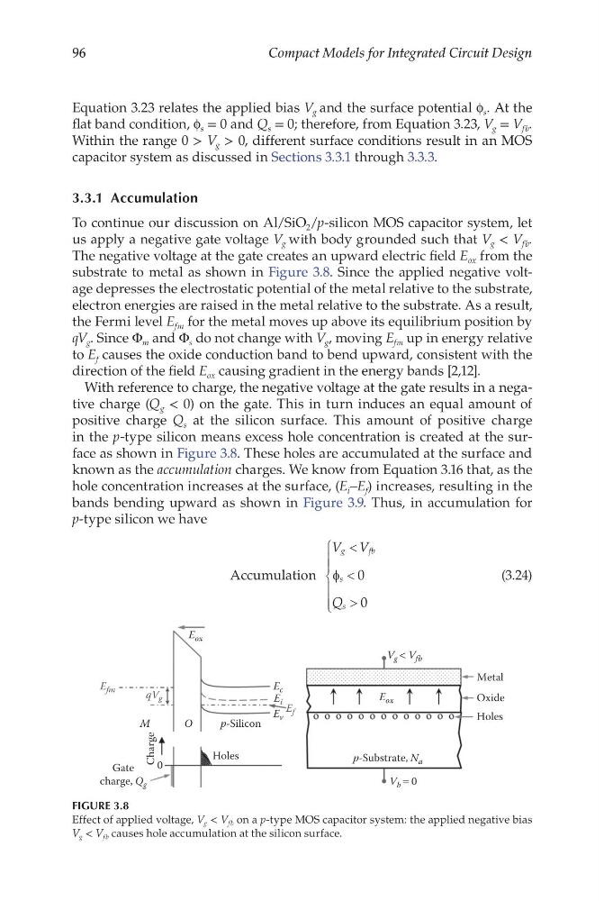
substrate to metal as shown in Figure 3.8. Since the applied negative voltage depresses the electrostatic potential of the metal relative to the substrate,
electron energies are raised in the metal relative to the substrate. As a result,
the Fermi level E fm for the metal moves up above its equilibrium position by
qV g . Since Φ m and Φ s do not change with V g , moving E fm up in energy relative
to E f causes the oxide conduction band to bend upward, consistent with the
direction of the field E ox causing gradient in the energy bands [2,12].
With reference to charge, the negative voltage at the gate results in a negative charge (Q g < 0) on the gate. This in turn induces an equal amount of
positive charge Q s at the silicon surface. This amount of positive charge
in the p-type silicon means excess hole concentration is created at the surface as shown in Figure 3.8. These holes are accumulated at the surface and
known as the accumulation charges. We know from Equation 3.16 that, as the
hole concentration increases at the surface, (E i –E f ) increases, resulting in the
bands bending upward as shown in Figure 3.9. Thus, in accumulation for
p-type silicon we have
Accumulation
V V
Q
g
f b
s
s
<
<
>
,
φ 0
0
(3.24)
Gate
charge, Q g
Holes
p-Silicon
p-Substrate, N a
E ox
E c
E ox
V g < V fb
V b = 0
E fm
E f
qV g
E v
E i
O
0
M
Holes
Oxide
Metal
Charge
FIGURE 3.8
Effect of applied voltage, V g < V fb on a p-type MOS capacitor system: the applied negative bias
V g < V fb causes hole accumulation at the silicon surface.
Compact Models for Integrated Circuit Design
Equation 3.23 relates the applied bias V g and the surface potential f s . At the
flat band condition, f s = 0 and Q s = 0; therefore, from Equation 3.23, V g = V fb .
Within the range 0 > V g > 0, different surface conditions result in an MOS
capacitor system as discussed in Sections 3.3.1 through 3.3.3.
3.3.1 Accumulation
To continue our discussion on Al/SiO 2 /p-silicon MOS capacitor system, let
us apply a negative gate voltage V g with body grounded such that V g < V fb .
The negative voltage at the gate creates an upward electric field E ox from the
substrate to metal as shown in Figure 3.8. Since the applied negative voltage depresses the electrostatic potential of the metal relative to the substrate,
electron energies are raised in the metal relative to the substrate. As a result,
the Fermi level E fm for the metal moves up above its equilibrium position by
qV g . Since Φ m and Φ s do not change with V g , moving E fm up in energy relative
to E f causes the oxide conduction band to bend upward, consistent with the
direction of the field E ox causing gradient in the energy bands [2,12].
With reference to charge, the negative voltage at the gate results in a negative charge (Q g < 0) on the gate. This in turn induces an equal amount of
positive charge Q s at the silicon surface. This amount of positive charge
in the p-type silicon means excess hole concentration is created at the surface as shown in Figure 3.8. These holes are accumulated at the surface and
known as the accumulation charges. We know from Equation 3.16 that, as the
hole concentration increases at the surface, (E i –E f ) increases, resulting in the
bands bending upward as shown in Figure 3.9. Thus, in accumulation for
p-type silicon we have
Accumulation
V V
Q
g
f b
s
s
<
<
>
,
φ 0
0
(3.24)
Gate
charge, Q g
Holes
p-Silicon
p-Substrate, N a
E ox
E c
E ox
V g < V fb
V b = 0
E fm
E f
qV g
E v
E i
O
0
M
Holes
Oxide
Metal
Charge
FIGURE 3.8
Effect of applied voltage, V g < V fb on a p-type MOS capacitor system: the applied negative bias
V g < V fb causes hole accumulation at the silicon surface.