

94
Compact Models for Integrated Circuit Design
The band bending described earlier can be compensated by applying an
external gate voltage given by Equation 3.15. The condition to achieve the flat
bands at the surface is called the flat band condition and the corresponding
gate voltage required to achieve the flat band condition is called the flat band
voltage, V fb . Thus, V fb is the applied gate voltage to have zero surface potential with
flat energy bands over the entire semiconductor surface. The flat band condition
is often used as a reference state along with V fb as a reference voltage and,
thus, can be considered as an important figure of merit for an MOS capacitor
system.
3.3 MOS Capacitor under Applied Bias
In the previous section, we described the behavior of an MOS capacitor
system without the application of any external bias. Now, let us discuss the
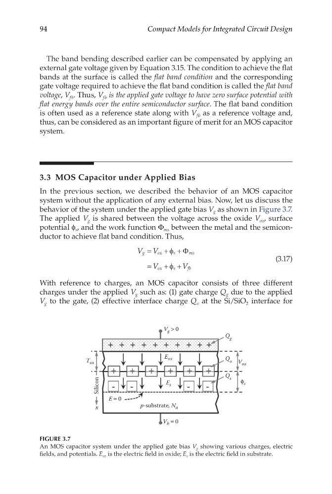
behavior of the system under the applied gate bias V g as shown in Figure 3.7.
The applied V g is shared between the voltage across the oxide V ox , surface
potential f s , and the work function Φ ms between the metal and the semiconductor to achieve flat band condition. Thus,
V V
V
V
g
o x
s
ms
ox
s
f b
=
+ +
=
+ +
φ
φ
Φ
(3.17)
With reference to charges, an MOS capacitor consists of three different
charges under the applied V g such as: (1) gate charge Q g due to the applied
V g to the gate, (2) effective interface charge Q o at the Si/SiO 2 interface for
T ox
E ox
E s
E = 0
p-substrate, N a
x
V g > 0
V b = 0
Q g
Silicon
Q s
Q o V ox
ϕ s
FIGURE 3.7
An MOS capacitor system under the applied gate bias V g showing various charges, electric
fields, and potentials. E ox is the electric field in oxide; E s is the electric field in substrate.
Compact Models for Integrated Circuit Design
The band bending described earlier can be compensated by applying an
external gate voltage given by Equation 3.15. The condition to achieve the flat
bands at the surface is called the flat band condition and the corresponding
gate voltage required to achieve the flat band condition is called the flat band
voltage, V fb . Thus, V fb is the applied gate voltage to have zero surface potential with
flat energy bands over the entire semiconductor surface. The flat band condition
is often used as a reference state along with V fb as a reference voltage and,
thus, can be considered as an important figure of merit for an MOS capacitor
system.
3.3 MOS Capacitor under Applied Bias
In the previous section, we described the behavior of an MOS capacitor
system without the application of any external bias. Now, let us discuss the
behavior of the system under the applied gate bias V g as shown in Figure 3.7.
The applied V g is shared between the voltage across the oxide V ox , surface
potential f s , and the work function Φ ms between the metal and the semiconductor to achieve flat band condition. Thus,
V V
V
V
g
o x
s
ms
ox
s
f b
=
+ +
=
+ +
φ
φ
Φ
(3.17)
With reference to charges, an MOS capacitor consists of three different
charges under the applied V g such as: (1) gate charge Q g due to the applied
V g to the gate, (2) effective interface charge Q o at the Si/SiO 2 interface for
T ox
E ox
E s
E = 0
p-substrate, N a
x
V g > 0
V b = 0
Q g
Silicon
Q s
Q o V ox
ϕ s
FIGURE 3.7
An MOS capacitor system under the applied gate bias V g showing various charges, electric
fields, and potentials. E ox is the electric field in oxide; E s is the electric field in substrate.