

93
Metal-Oxide-Semiconductor System
3.2.4 Effect of Band Bending on the Semiconductor Surface
Let us now consider an Al-SiO 2 -Si MOS capacitor system on a p-type substrate to discuss the effect of band bending at the silicon surface on the
surface behavior of MOS capacitors. We know that the concentration of holes
in a p-type substrate is given by (Equation 2.63),
p n
E E
kT
i
i
f
=
−
exp
(3.16)
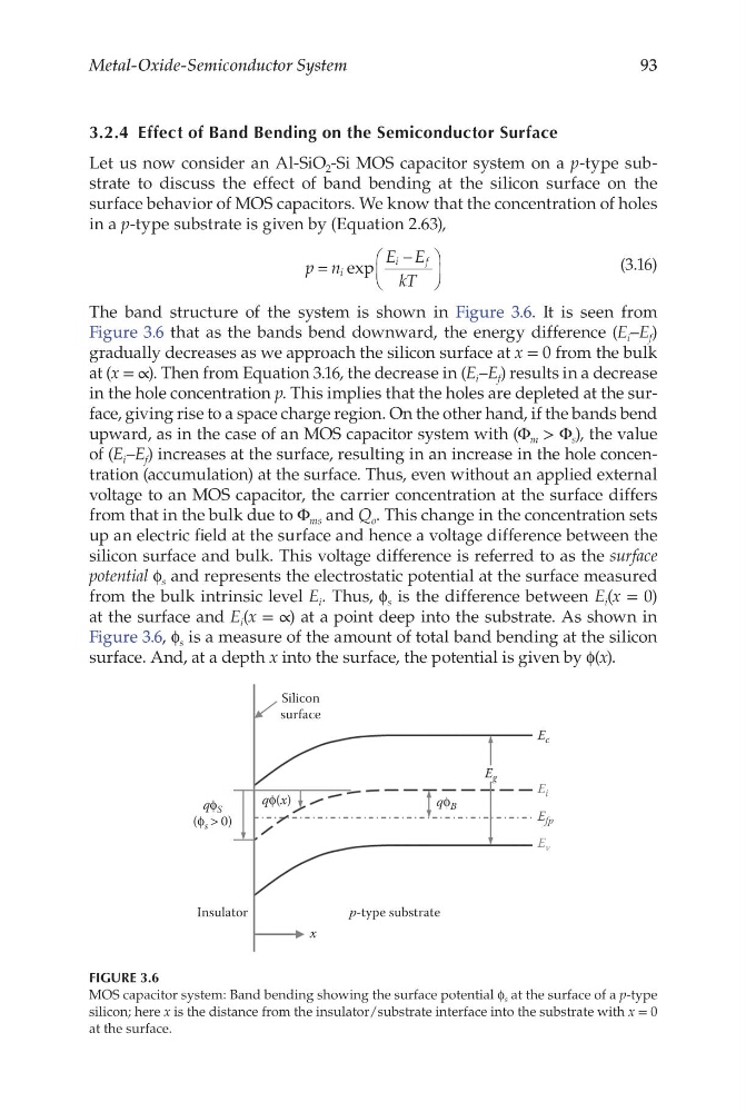
The band structure of the system is shown in Figure 3.6. It is seen from
Figure 3.6 that as the bands bend downward, the energy difference (E i –E f )
gradually decreases as we approach the silicon surface at x = 0 from the bulk
at (x = ∝). Then from Equation 3.16, the decrease in (E i –E f ) results in a decrease
in the hole concentration p. This implies that the holes are depleted at the surface, giving rise to a space charge region. On the other hand, if the bands bend
upward, as in the case of an MOS capacitor system with (Φ m > Φ s ), the value
of (E i –E f ) increases at the surface, resulting in an increase in the hole concentration (accumulation) at the surface. Thus, even without an applied external
voltage to an MOS capacitor, the carrier concentration at the surface differs
from that in the bulk due to Φ ms and Q o . This change in the concentration sets
up an electric field at the surface and hence a voltage difference between the
silicon surface and bulk. This voltage difference is referred to as the surface
potential f s and represents the electrostatic potential at the surface measured
from the bulk intrinsic level E i . Thus, f s is the difference between E i (x = 0)
at the surface and E i (x = ∝) at a point deep into the substrate. As shown in
Figure 3.6, f s is a measure of the amount of total band bending at the silicon
surface. And, at a depth x into the surface, the potential is given by f(x).
Silicon
surface
Insulator
x
p-type substrate
E c
E g
qϕ B
qϕ(x)
qϕ S
(ϕ s > 0)
E i
E fp
E v
FIGURE 3.6
MOS capacitor system: Band bending showing the surface potential f s at the surface of a p-type
silicon; here x is the distance from the insulator/substrate interface into the substrate with x = 0
at the surface.
Metal-Oxide-Semiconductor System
3.2.4 Effect of Band Bending on the Semiconductor Surface
Let us now consider an Al-SiO 2 -Si MOS capacitor system on a p-type substrate to discuss the effect of band bending at the silicon surface on the
surface behavior of MOS capacitors. We know that the concentration of holes
in a p-type substrate is given by (Equation 2.63),
p n
E E
kT
i
i
f
=
−
exp
(3.16)
The band structure of the system is shown in Figure 3.6. It is seen from
Figure 3.6 that as the bands bend downward, the energy difference (E i –E f )
gradually decreases as we approach the silicon surface at x = 0 from the bulk
at (x = ∝). Then from Equation 3.16, the decrease in (E i –E f ) results in a decrease
in the hole concentration p. This implies that the holes are depleted at the surface, giving rise to a space charge region. On the other hand, if the bands bend
upward, as in the case of an MOS capacitor system with (Φ m > Φ s ), the value
of (E i –E f ) increases at the surface, resulting in an increase in the hole concentration (accumulation) at the surface. Thus, even without an applied external
voltage to an MOS capacitor, the carrier concentration at the surface differs
from that in the bulk due to Φ ms and Q o . This change in the concentration sets
up an electric field at the surface and hence a voltage difference between the
silicon surface and bulk. This voltage difference is referred to as the surface
potential f s and represents the electrostatic potential at the surface measured
from the bulk intrinsic level E i . Thus, f s is the difference between E i (x = 0)
at the surface and E i (x = ∝) at a point deep into the substrate. As shown in
Figure 3.6, f s is a measure of the amount of total band bending at the silicon
surface. And, at a depth x into the surface, the potential is given by f(x).
Silicon
surface
Insulator
x
p-type substrate
E c
E g
qϕ B
qϕ(x)
qϕ S
(ϕ s > 0)
E i
E fp
E v
FIGURE 3.6
MOS capacitor system: Band bending showing the surface potential f s at the surface of a p-type
silicon; here x is the distance from the insulator/substrate interface into the substrate with x = 0
at the surface.