

92
Compact Models for Integrated Circuit Design
3.2.3 Flat Band Voltage
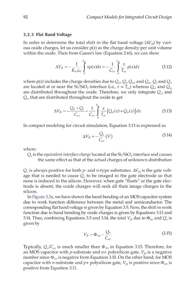
In order to determine the total shift in the flat band voltage (ΔV fb ) by various oxide charges, let us consider ρ(x) as the charge density per unit volume
within the oxide. Then from Gauss’s law (Equation 2.61), we can show
∆V
K
x x dx
C
x
T
x dx
fb
ox
T
ox
ox
T
ox
ox
= −
= −
∫
∫
1
1
0 0
0
ε
ρ
ρ
( )
( )
(3.12)
where ρ(x) includes the charge densities due to Q it , Q f , Q ot , and Q m . Q f and Q it
are located at or near the Si/SiO 2 interface (i.e., x = T ox ) whereas Q ot and Q m
are distributed throughout the oxide. Therefore, we only integrate Q ot and
Q m that are distributed throughout the oxide to get
∆V
Q Q
C
C
x
T
Q x Q x dx
fb
it
f
ox
ox
ox
ot
m
Tox
= −
+
−
+
[
]
∫
1
0
( )
( )
(3.13)
In compact modeling for circuit simulation, Equation 3.13 is expressed as
∆V
Q
C
V
fb
o
ox
= −
( )
(3.14)
where:
Q o is the equivalent interface charge located at the Si/SiO 2 interface and causes
the same effect as that of the actual charges of unknown distribution
Q o is always positive for both p- and n-type substrates. ΔV fb is the gate voltage that is needed to cause Q o to be imaged in the gate electrode so that
none is induced in the silicon. However, when gate “floats” or the gate electrode is absent, the oxide charges will seek all their image charges in the
silicon.
In Figure 3.3a, we have shown the band bending of an MOS capacitor system
due to work function difference between the metal and semiconductor. The
corresponding flat band voltage is given by Equation 3.5. Now, the shift in work
function due to band bending by oxide charges is given by Equations 3.13 and
3.14. Thus, combining Equations 3.5 and 3.14, the total V fb due to Φ ms and Q o is
given by
V
Q
C
fb
ms
o
ox
=
−
Φ
(3.15)
Typically, Q o /C ox is much smaller than Φ ms in Equation 3.15. Therefore, for
an MOS capacitor with p-substrate and n+ polysilicon gate, V fb is a negative
number since Φ ms is negative from Equation 3.10. On the other hand, for MOS
capacitor with n-substrate and p+ polysilicon gate, V fb is positive since Φ ms is
positive from Equation 3.11.
Compact Models for Integrated Circuit Design
3.2.3 Flat Band Voltage
In order to determine the total shift in the flat band voltage (ΔV fb ) by various oxide charges, let us consider ρ(x) as the charge density per unit volume
within the oxide. Then from Gauss’s law (Equation 2.61), we can show
∆V
K
x x dx
C
x
T
x dx
fb
ox
T
ox
ox
T
ox
ox
= −
= −
∫
∫
1
1
0 0
0
ε
ρ
ρ
( )
( )
(3.12)
where ρ(x) includes the charge densities due to Q it , Q f , Q ot , and Q m . Q f and Q it
are located at or near the Si/SiO 2 interface (i.e., x = T ox ) whereas Q ot and Q m
are distributed throughout the oxide. Therefore, we only integrate Q ot and
Q m that are distributed throughout the oxide to get
∆V
Q Q
C
C
x
T
Q x Q x dx
fb
it
f
ox
ox
ox
ot
m
Tox
= −
+
−
+
[
]
∫
1
0
( )
( )
(3.13)
In compact modeling for circuit simulation, Equation 3.13 is expressed as
∆V
Q
C
V
fb
o
ox
= −
( )
(3.14)
where:
Q o is the equivalent interface charge located at the Si/SiO 2 interface and causes
the same effect as that of the actual charges of unknown distribution
Q o is always positive for both p- and n-type substrates. ΔV fb is the gate voltage that is needed to cause Q o to be imaged in the gate electrode so that
none is induced in the silicon. However, when gate “floats” or the gate electrode is absent, the oxide charges will seek all their image charges in the
silicon.
In Figure 3.3a, we have shown the band bending of an MOS capacitor system
due to work function difference between the metal and semiconductor. The
corresponding flat band voltage is given by Equation 3.5. Now, the shift in work
function due to band bending by oxide charges is given by Equations 3.13 and
3.14. Thus, combining Equations 3.5 and 3.14, the total V fb due to Φ ms and Q o is
given by
V
Q
C
fb
ms
o
ox
=
−
Φ
(3.15)
Typically, Q o /C ox is much smaller than Φ ms in Equation 3.15. Therefore, for
an MOS capacitor with p-substrate and n+ polysilicon gate, V fb is a negative
number since Φ ms is negative from Equation 3.10. On the other hand, for MOS
capacitor with n-substrate and p+ polysilicon gate, V fb is positive since Φ ms is
positive from Equation 3.11.