

Microprocessors
543
CLK OUT
READY
ALE SO
S1 IO/M
HOLD
HLDA
RESET OUT
AD -AD
ADDRESS/DATA BUS
7
0
A -A
ADDRESS BUS
15
8
Address Buffer
Address/
Data Buffer
(8)
(8)
+5V
GND
X1
X2
Timing and Control
Arithmetic
logic
unit
(ALU)
Instruction
decoder
and
machine
cycle
encoding
Flag
flip-flops
Instruction
register
(8)
Temp. reg.
(8)
(8)
Aaccumulator
B
Reg
D
Reg
H
Reg
C
Reg
E
Reg
L
Reg
(8)
(8)
(8)
(8)
(8)
(8)
Stack
Pointer
Program
Counter
Incrementer/
Decrementer Address Latch
(16)
(16)
(16)
Interrupt Control
Serial I/O
Control
8-bit internal data bus
INTR INTA
RST 5.5
RST 6.5
RST 7.5
TRAP
SID
SOD
(5)
(8)
{
Power
supply
r
e
t
s i
g
e
R y
a r
r
a
RESETIN
RD
WR
CLK
GEN
CONTROL
STATUS
DMA
RESET
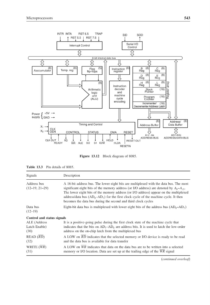
Figure 13.12 Block diagram of 8085.
Table 13.3 Pin details of 8085.
Signals
Description
Address bus
(12–19, 21–29)
A 16-bit address bus. The lower eight bits are multiplexed with the data bus. The most
significant eight bits of the memory address (or I/O address) are denoted by A 8 –A 15 .
The lower eight bits of the memory address (or I/O address) appear on the multiplexed
address/data bus (AD 0 –AD 7 for the first clock cycle of the machine cycle. It then
becomes the data bus during the second and third clock cycles
Data bus
(12–19)
Eight-bit data bus is multiplexed with lower eight bits of the address bus (AD 0 –AD 7
Control and status signals
ALE (Address
Latch Enable)
(30)
It is a positive-going pulse during the first clock state of the machine cycle that
indicates that the bits on AD 7 –AD 0 are address bits. It is used to latch the low-order
address on the on-chip latch from the multiplexed bus
READ (RDD
(32)
A LOW on RD indicates that the selected memory or I/O device is ready to be read
and the data bus is available for data transfer
WRITE (WRR
(31)
A LOW on WR indicates that data on the data bus are to be written into a selected
memory or I/O location. Data are set up at the trailing edge of the WR signal
(continued overleaf)
543
CLK OUT
READY
ALE SO
S1 IO/M
HOLD
HLDA
RESET OUT
AD -AD
ADDRESS/DATA BUS
7
0
A -A
ADDRESS BUS
15
8
Address Buffer
Address/
Data Buffer
(8)
(8)
+5V
GND
X1
X2
Timing and Control
Arithmetic
logic
unit
(ALU)
Instruction
decoder
and
machine
cycle
encoding
Flag
flip-flops
Instruction
register
(8)
Temp. reg.
(8)
(8)
Aaccumulator
B
Reg
D
Reg
H
Reg
C
Reg
E
Reg
L
Reg
(8)
(8)
(8)
(8)
(8)
(8)
Stack
Pointer
Program
Counter
Incrementer/
Decrementer Address Latch
(16)
(16)
(16)
Interrupt Control
Serial I/O
Control
8-bit internal data bus
INTR INTA
RST 5.5
RST 6.5
RST 7.5
TRAP
SID
SOD
(5)
(8)
{
Power
supply
r
e
t
s i
g
e
R y
a r
r
a
RESETIN
RD
WR
CLK
GEN
CONTROL
STATUS
DMA
RESET
Figure 13.12 Block diagram of 8085.
Table 13.3 Pin details of 8085.
Signals
Description
Address bus
(12–19, 21–29)
A 16-bit address bus. The lower eight bits are multiplexed with the data bus. The most
significant eight bits of the memory address (or I/O address) are denoted by A 8 –A 15 .
The lower eight bits of the memory address (or I/O address) appear on the multiplexed
address/data bus (AD 0 –AD 7 for the first clock cycle of the machine cycle. It then
becomes the data bus during the second and third clock cycles
Data bus
(12–19)
Eight-bit data bus is multiplexed with lower eight bits of the address bus (AD 0 –AD 7
Control and status signals
ALE (Address
Latch Enable)
(30)
It is a positive-going pulse during the first clock state of the machine cycle that
indicates that the bits on AD 7 –AD 0 are address bits. It is used to latch the low-order
address on the on-chip latch from the multiplexed bus
READ (RDD
(32)
A LOW on RD indicates that the selected memory or I/O device is ready to be read
and the data bus is available for data transfer
WRITE (WRR
(31)
A LOW on WR indicates that data on the data bus are to be written into a selected
memory or I/O location. Data are set up at the trailing edge of the WR signal
(continued overleaf)