

518
Digital Electronics
Gated
Clock
SAR
21
19
1
3
12
13
17
DAC
27
18
REF
6.3K
5K
5K
25
30
23
29
24
22
26
20
32
31
14
16
15
+
−
Clock
Out
LSB
MSB
Status
Serial Out
MSB
Digital
GND
Analog
GND
Comp IN
10V Span
20V Span
Bipolar
Offset
Ref
Out
Gain
ADJ
Clock Rate
Control
Convert
Command
Comparator
28
AD ADC84
AD ADC84
+5V
+V s
Short
Cycle
−V s
Buffer
Out
Buffer
In
+
−
(12Bit)
LSB (10Bit)
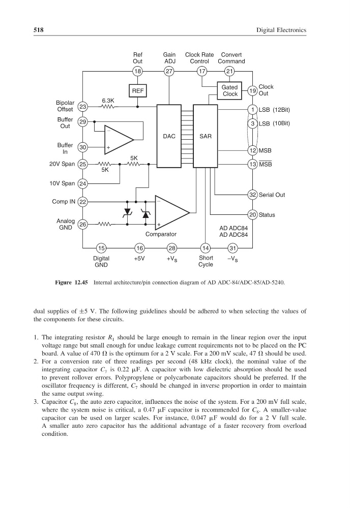
Figure 12.45 Internal architecture/pin connection diagram of AD ADC-84/ADC-85/AD-5240.
dual supplies of ±5 V. The following guidelines should be adhered to when selecting the values of
the components for these circuits.
1. The integrating resistor R 1 should be large enough to remain in the linear region over the input
voltage range but small enough for undue leakage current requirements not to be placed on the PC
board. A value of 470 is the optimum for a 2 V scale. For a 200 mV scale, 47 should be used.
2. For a conversion rate of three readings per second (48 kHz clock), the nominal value of the
integrating capacitor C 7 is 0.22 F. A capacitor with low dielectric absorption should be used
to prevent rollover errors. Polypropylene or polycarbonate capacitors should be preferred. If the
oscillator frequency is different, C 7 should be changed in inverse proportion in order to maintain
the same output swing.
3. Capacitor C 8 , the auto zero capacitor, influences the noise of the system. For a 200 mV full scale,
where the system noise is critical, a 0.47 F capacitor is recommended for C 8 . A smaller-value
capacitor can be used on larger scales. For instance, 0.047 F would do for a 2 V full scale.
A smaller auto zero capacitor has the additional advantage of a faster recovery from overload
condition.
Digital Electronics
Gated
Clock
SAR
21
19
1
3
12
13
17
DAC
27
18
REF
6.3K
5K
5K
25
30
23
29
24
22
26
20
32
31
14
16
15
+
−
Clock
Out
LSB
MSB
Status
Serial Out
MSB
Digital
GND
Analog
GND
Comp IN
10V Span
20V Span
Bipolar
Offset
Ref
Out
Gain
ADJ
Clock Rate
Control
Convert
Command
Comparator
28
AD ADC84
AD ADC84
+5V
+V s
Short
Cycle
−V s
Buffer
Out
Buffer
In
+
−
(12Bit)
LSB (10Bit)
Figure 12.45 Internal architecture/pin connection diagram of AD ADC-84/ADC-85/AD-5240.
dual supplies of ±5 V. The following guidelines should be adhered to when selecting the values of
the components for these circuits.
1. The integrating resistor R 1 should be large enough to remain in the linear region over the input
voltage range but small enough for undue leakage current requirements not to be placed on the PC
board. A value of 470 is the optimum for a 2 V scale. For a 200 mV scale, 47 should be used.
2. For a conversion rate of three readings per second (48 kHz clock), the nominal value of the
integrating capacitor C 7 is 0.22 F. A capacitor with low dielectric absorption should be used
to prevent rollover errors. Polypropylene or polycarbonate capacitors should be preferred. If the
oscillator frequency is different, C 7 should be changed in inverse proportion in order to maintain
the same output swing.
3. Capacitor C 8 , the auto zero capacitor, influences the noise of the system. For a 200 mV full scale,
where the system noise is critical, a 0.47 F capacitor is recommended for C 8 . A smaller-value
capacitor can be used on larger scales. For instance, 0.047 F would do for a 2 V full scale.
A smaller auto zero capacitor has the additional advantage of a faster recovery from overload
condition.