

516
Digital Electronics
8 Analog
Inputs
8 Channels
Multiplexing
Analog
Switches
TriState
Output
Latch
Buffer
S.A.R
Control&
Timming
Switch
Tree
256R Resistor
Ladder
Clock
Start
Comparator
Address
Latch
And
Decoder
8-Bit A/D
V CC GND REF(+)
REF(-)
Output
Enable
End Of Conversion
(Interrupt)
8-Bit
Outputs
3-Bit
Address
Address
Latch Enable
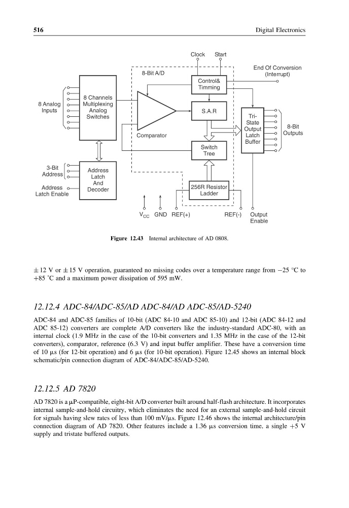
Figure 12.43 Internal architecture of AD 0808.
± 12 V or ± 15 V operation, guaranteed no missing codes over a temperature range from −25 °C to
+85 ˚C and a maximum power dissipation of 595 mW.
12.12.4 ADC-84/ADC-85/AD ADC-84/AD ADC-85/AD-5240
ADC-84 and ADC-85 families of 10-bit (ADC 84-10 and ADC 85-10) and 12-bit (ADC 84-12 and
ADC 85-12) converters are complete A/D converters like the industry-standard ADC-80, with an
internal clock (1.9 MHz in the case of the 10-bit converters and 1.35 MHz in the case of the 12-bit
converters), comparator, reference (6.3 V) and input buffer amplifier. These have a conversion time
of 10 s (for 12-bit operation) and 6 s (for 10-bit operation). Figure 12.45 shows an internal block
schematic/pin connection diagram of ADC-84/ADC-85/AD-5240.
12.12.5 AD 7820
AD 7820 is a P-compatible, eight-bit A/D converter built around half-flash architecture. It incorporates
internal sample-and-hold circuitry, which eliminates the need for an external sample-and-hold circuit
for signals having slew rates of less than 100 mV/s. Figure 12.46 shows the internal architecture/pin
connection diagram of AD 7820. Other features include a 1.36 s conversion time, a single +5 V
supply and tristate buffered outputs.
Digital Electronics
8 Analog
Inputs
8 Channels
Multiplexing
Analog
Switches
TriState
Output
Latch
Buffer
S.A.R
Control&
Timming
Switch
Tree
256R Resistor
Ladder
Clock
Start
Comparator
Address
Latch
And
Decoder
8-Bit A/D
V CC GND REF(+)
REF(-)
Output
Enable
End Of Conversion
(Interrupt)
8-Bit
Outputs
3-Bit
Address
Address
Latch Enable
Figure 12.43 Internal architecture of AD 0808.
± 12 V or ± 15 V operation, guaranteed no missing codes over a temperature range from −25 °C to
+85 ˚C and a maximum power dissipation of 595 mW.
12.12.4 ADC-84/ADC-85/AD ADC-84/AD ADC-85/AD-5240
ADC-84 and ADC-85 families of 10-bit (ADC 84-10 and ADC 85-10) and 12-bit (ADC 84-12 and
ADC 85-12) converters are complete A/D converters like the industry-standard ADC-80, with an
internal clock (1.9 MHz in the case of the 10-bit converters and 1.35 MHz in the case of the 12-bit
converters), comparator, reference (6.3 V) and input buffer amplifier. These have a conversion time
of 10 s (for 12-bit operation) and 6 s (for 10-bit operation). Figure 12.45 shows an internal block
schematic/pin connection diagram of ADC-84/ADC-85/AD-5240.
12.12.5 AD 7820
AD 7820 is a P-compatible, eight-bit A/D converter built around half-flash architecture. It incorporates
internal sample-and-hold circuitry, which eliminates the need for an external sample-and-hold circuit
for signals having slew rates of less than 100 mV/s. Figure 12.46 shows the internal architecture/pin
connection diagram of AD 7820. Other features include a 1.36 s conversion time, a single +5 V
supply and tristate buffered outputs.