

Data Conversion Circuits – D/A and A/D Converters
515
15 10 18 8
11
7
6
9
5 12
ADC 0800
+5V
-5V V in
Output
Enable
SC
EOC
8-Bit
Word
(a)
15 10 8
12
7
6
9
5 18
ADC 0800
+10V
Output
Enable
SC
EOC
8-Bit
Word
(b)
-12V Clock
-7V
V in
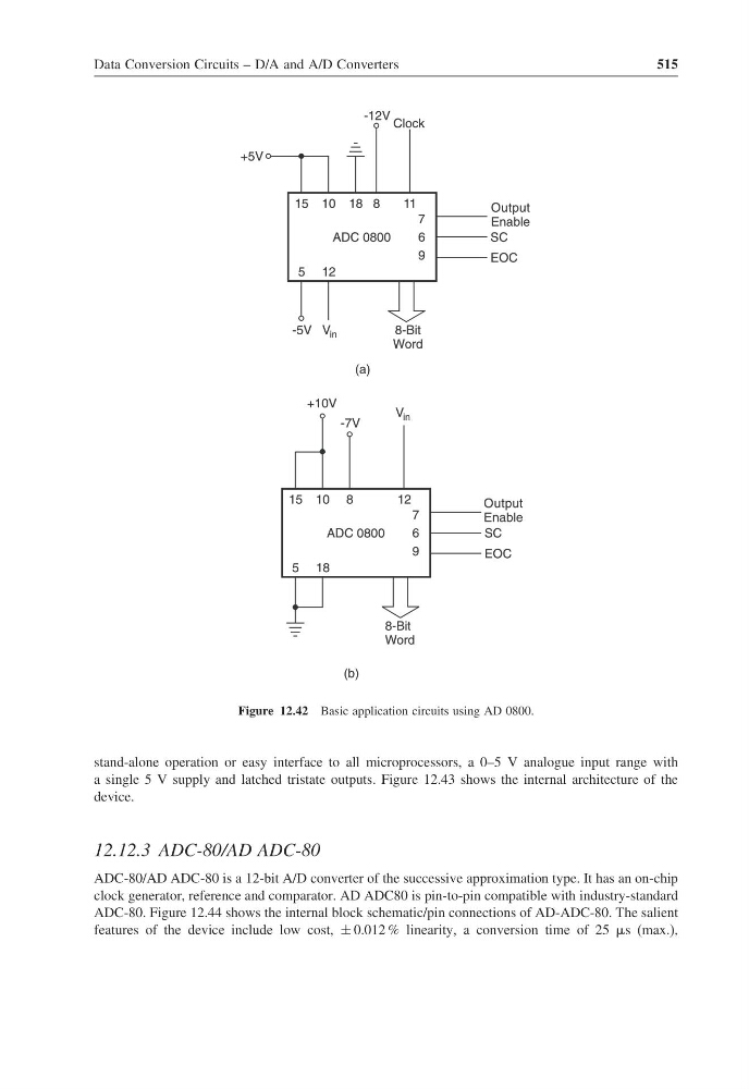
Figure 12.42 Basic application circuits using AD 0800.
stand-alone operation or easy interface to all microprocessors, a 0–5 V analogue input range with
a single 5 V supply and latched tristate outputs. Figure 12.43 shows the internal architecture of the
device.
12.12.3 ADC-80/AD ADC-80
ADC-80/AD ADC-80 is a 12-bit A/D converter of the successive approximation type. It has an on-chip
clock generator, reference and comparator. AD ADC80 is pin-to-pin compatible with industry-standard
ADC-80. Figure 12.44 shows the internal block schematic/pin connections of AD-ADC-80. The salient
features of the device include low cost, ± 0.012 % linearity, a conversion time of 25 s (max.),
515
15 10 18 8
11
7
6
9
5 12
ADC 0800
+5V
-5V V in
Output
Enable
SC
EOC
8-Bit
Word
(a)
15 10 8
12
7
6
9
5 18
ADC 0800
+10V
Output
Enable
SC
EOC
8-Bit
Word
(b)
-12V Clock
-7V
V in
Figure 12.42 Basic application circuits using AD 0800.
stand-alone operation or easy interface to all microprocessors, a 0–5 V analogue input range with
a single 5 V supply and latched tristate outputs. Figure 12.43 shows the internal architecture of the
device.
12.12.3 ADC-80/AD ADC-80
ADC-80/AD ADC-80 is a 12-bit A/D converter of the successive approximation type. It has an on-chip
clock generator, reference and comparator. AD ADC80 is pin-to-pin compatible with industry-standard
ADC-80. Figure 12.44 shows the internal block schematic/pin connections of AD-ADC-80. The salient
features of the device include low cost, ± 0.012 % linearity, a conversion time of 25 s (max.),