

Data Conversion Circuits – D/A and A/D Converters
475
contribute 2V/(2
n
− 1) to the output. The contributions of successive higher bit positions in the case
of a logic ‘1’ would be 4V/(2
n
− 1), 8V/(2
n
− 1), 16V/(2
n
− 1) and so on. That is, the contribution of
any given bit position owing to the presence of a logic ‘1’ is twice the contribution of the adjacent
lower bit position and half that of the adjacent higher bit position. When all input bit positions have a
logic ‘1’, the analogue output is given by
V A =
VV2
0
+ 2
1
+ 2
2
+ · · · + 2
n−1
2 n − 1
= V
(12.6)
In the case of all inputs being in the logic ‘0’ state, V A = 0. Therefore, the analogue output varies from
0 to V volts as the digital input varies from an all 0s to an all 1s input.
12.1.2 Binary Ladder Network for D/A Conversion
The simple resistive divider network of Fig. 12.1 has two serious drawbacks. One, each resistor in
the network is of a different value. Since these networks use precision resistors, the added expense
becomes unattractive. Two, the resistor used for the most significant bit (MSB) is required to handle
a much larger current than the LSB resistor. For example, in a 10-bit network, the current through the
MSB resistor will be about 500 times the current through the LSB resistor.
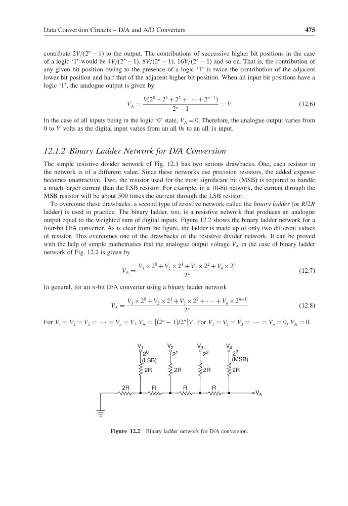
To overcome these drawbacks, a second type of resistive network called the binary ladder (or R/2R
ladder) is used in practice. The binary ladder, too, is a resistive network that produces an analogue
output equal to the weighted sum of digital inputs. Figure 12.2 shows the binary ladder network for a
four-bit D/A converter. As is clear from the figure, the ladder is made up of only two different values
of resistor. This overcomes one of the drawbacks of the resistive divider network. It can be proved
with the help of simple mathematics that the analogue output voltage V A in the case of binary ladder
network of Fig. 12.2 is given by
V A =
V 1 × 2
0
+ V 2 × 2
1
+ V 3 × 2
2
+ V 4 × 2
3
2 4
(12.7)
In general, for an n-bit D/A converter using a binary ladder network
V A =
V 1 × 2
0
+ V 2 × 2
1
+ V 3 × 2
2
+ · · · + V n × 2
n−1
2 n
(12.8)
For V 1 = V 2 = V 3 = · · · = V n = V , V A = [(2
n
− 1)/2
n ]V . For V 1 = V 2 = V 3 = · · · = V n = 0, V A = 0.
V 3
V 2
2R
V 1
V A
R
R
R
V 4
2R
2R
2R
2R
2
0
2
1
2
2
2
3
(MSB)
(LSB)
Figure 12.2 Binary ladder network for D/A conversion.
475
contribute 2V/(2
n
− 1) to the output. The contributions of successive higher bit positions in the case
of a logic ‘1’ would be 4V/(2
n
− 1), 8V/(2
n
− 1), 16V/(2
n
− 1) and so on. That is, the contribution of
any given bit position owing to the presence of a logic ‘1’ is twice the contribution of the adjacent
lower bit position and half that of the adjacent higher bit position. When all input bit positions have a
logic ‘1’, the analogue output is given by
V A =
VV2
0
+ 2
1
+ 2
2
+ · · · + 2
n−1
2 n − 1
= V
(12.6)
In the case of all inputs being in the logic ‘0’ state, V A = 0. Therefore, the analogue output varies from
0 to V volts as the digital input varies from an all 0s to an all 1s input.
12.1.2 Binary Ladder Network for D/A Conversion
The simple resistive divider network of Fig. 12.1 has two serious drawbacks. One, each resistor in
the network is of a different value. Since these networks use precision resistors, the added expense
becomes unattractive. Two, the resistor used for the most significant bit (MSB) is required to handle
a much larger current than the LSB resistor. For example, in a 10-bit network, the current through the
MSB resistor will be about 500 times the current through the LSB resistor.
To overcome these drawbacks, a second type of resistive network called the binary ladder (or R/2R
ladder) is used in practice. The binary ladder, too, is a resistive network that produces an analogue
output equal to the weighted sum of digital inputs. Figure 12.2 shows the binary ladder network for a
four-bit D/A converter. As is clear from the figure, the ladder is made up of only two different values
of resistor. This overcomes one of the drawbacks of the resistive divider network. It can be proved
with the help of simple mathematics that the analogue output voltage V A in the case of binary ladder
network of Fig. 12.2 is given by
V A =
V 1 × 2
0
+ V 2 × 2
1
+ V 3 × 2
2
+ V 4 × 2
3
2 4
(12.7)
In general, for an n-bit D/A converter using a binary ladder network
V A =
V 1 × 2
0
+ V 2 × 2
1
+ V 3 × 2
2
+ · · · + V n × 2
n−1
2 n
(12.8)
For V 1 = V 2 = V 3 = · · · = V n = V , V A = [(2
n
− 1)/2
n ]V . For V 1 = V 2 = V 3 = · · · = V n = 0, V A = 0.
V 3
V 2
2R
V 1
V A
R
R
R
V 4
2R
2R
2R
2R
2
0
2
1
2
2
2
3
(MSB)
(LSB)
Figure 12.2 Binary ladder network for D/A conversion.