

464
Digital Electronics
74164
CP
Clock
Q 0
Q 1
Q 2
Q 3
Q 4
Q 5
Q 6
Q 7
A
B
'1'
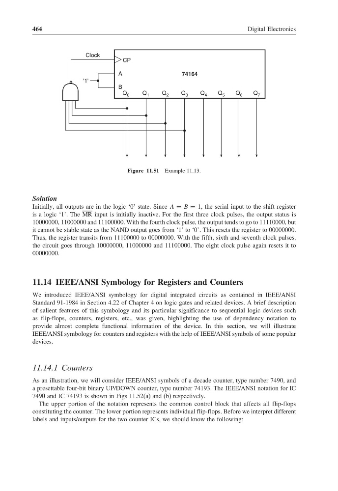
Figure 11.51 Example 11.13.
Solution
Initially, all outputs are in the logic ‘0’ state. Since A = B = 1, the serial input to the shift register
is a logic ‘1’. The MR input is initially inactive. For the first three clock pulses, the output status is
10000000, 11000000 and 11100000. With the fourth clock pulse, the output tends to go to 11110000, but
it cannot be stable state as the NAND output goes from ‘1’ to ‘0’. This resets the register to 00000000.
Thus, the register transits from 11100000 to 00000000. With the fifth, sixth and seventh clock pulses,
the circuit goes through 10000000, 11000000 and 11100000. The eight clock pulse again resets it to
00000000.
11.14 IEEE/ANSI Symbology for Registers and Counters
We introduced IEEE/ANSI symbology for digital integrated circuits as contained in IEEE/ANSI
Standard 91-1984 in Section 4.22 of Chapter 4 on logic gates and related devices. A brief description
of salient features of this symbology and its particular significance to sequential logic devices such
as flip-flops, counters, registers, etc., was given, highlighting the use of dependency notation to
provide almost complete functional information of the device. In this section, we will illustrate
IEEE/ANSI symbology for counters and registers with the help of IEEE/ANSI symbols of some popular
devices.
11.14.1 Counters
As an illustration, we will consider IEEE/ANSI symbols of a decade counter, type number 7490, and
a presettable four-bit binary UP/DOWN counter, type number 74193. The IEEE/ANSI notation for IC
7490 and IC 74193 is shown in Figs 11.52(a) and (b) respectively.
The upper portion of the notation represents the common control block that affects all flip-flops
constituting the counter. The lower portion represents individual flip-flops. Before we interpret different
labels and inputs/outputs for the two counter ICs, we should know the following:
Digital Electronics
74164
CP
Clock
Q 0
Q 1
Q 2
Q 3
Q 4
Q 5
Q 6
Q 7
A
B
'1'
Figure 11.51 Example 11.13.
Solution
Initially, all outputs are in the logic ‘0’ state. Since A = B = 1, the serial input to the shift register
is a logic ‘1’. The MR input is initially inactive. For the first three clock pulses, the output status is
10000000, 11000000 and 11100000. With the fourth clock pulse, the output tends to go to 11110000, but
it cannot be stable state as the NAND output goes from ‘1’ to ‘0’. This resets the register to 00000000.
Thus, the register transits from 11100000 to 00000000. With the fifth, sixth and seventh clock pulses,
the circuit goes through 10000000, 11000000 and 11100000. The eight clock pulse again resets it to
00000000.
11.14 IEEE/ANSI Symbology for Registers and Counters
We introduced IEEE/ANSI symbology for digital integrated circuits as contained in IEEE/ANSI
Standard 91-1984 in Section 4.22 of Chapter 4 on logic gates and related devices. A brief description
of salient features of this symbology and its particular significance to sequential logic devices such
as flip-flops, counters, registers, etc., was given, highlighting the use of dependency notation to
provide almost complete functional information of the device. In this section, we will illustrate
IEEE/ANSI symbology for counters and registers with the help of IEEE/ANSI symbols of some popular
devices.
11.14.1 Counters
As an illustration, we will consider IEEE/ANSI symbols of a decade counter, type number 7490, and
a presettable four-bit binary UP/DOWN counter, type number 74193. The IEEE/ANSI notation for IC
7490 and IC 74193 is shown in Figs 11.52(a) and (b) respectively.
The upper portion of the notation represents the common control block that affects all flip-flops
constituting the counter. The lower portion represents individual flip-flops. Before we interpret different
labels and inputs/outputs for the two counter ICs, we should know the following: