

Counters and Registers
463
A
B
C
D
E
5-Bit
Ring Counter
CP
CP JK
Flip Flop
F
1
F
Clock
A
B
C
D
E
J
K
LSB
MSB
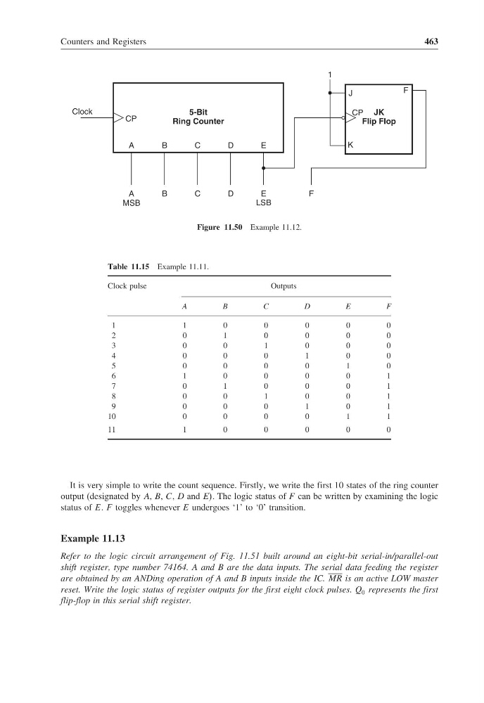
Figure 11.50 Example 11.12.
Table 11.15 Example 11.11.
Clock pulse
Outputs
A
B
C
D
E
F
1
1
0
0
0
0
0
2
0
1
0
0
0
0
3
0
0
1
0
0
0
4
0
0
0
1
0
0
5
0
0
0
0
1
0
6
1
0
0
0
0
1
7
0
1
0
0
0
1
8
0
0
1
0
0
1
9
0
0
0
1
0
1
1 0
0
0
0
0
1
1
1 1
1
0
0
0
0
0
It is very simple to write the count sequence. Firstly, we write the first 10 states of the ring counter
output (designated by A, B, C, D and EE. The logic status of F can be written by examining the logic
status of E. F toggles whenever E undergoes ‘1’ to ‘0’ transition.
Example 11.13
Refer to the logic circuit arrangement of Fig. 11.51 built around an eight-bit serial-in/parallel-out
shift register, type number 74164. A and B are the data inputs. The serial data feeding the register
are obtained by an ANDing operation of A and B inputs inside the IC. MR is an active LOW master
reset. Write the logic status of register outputs for the first eight clock pulses. Q 0 represents the first
flip-flop in this serial shift register.
463
A
B
C
D
E
5-Bit
Ring Counter
CP
CP JK
Flip Flop
F
1
F
Clock
A
B
C
D
E
J
K
LSB
MSB
Figure 11.50 Example 11.12.
Table 11.15 Example 11.11.
Clock pulse
Outputs
A
B
C
D
E
F
1
1
0
0
0
0
0
2
0
1
0
0
0
0
3
0
0
1
0
0
0
4
0
0
0
1
0
0
5
0
0
0
0
1
0
6
1
0
0
0
0
1
7
0
1
0
0
0
1
8
0
0
1
0
0
1
9
0
0
0
1
0
1
1 0
0
0
0
0
1
1
1 1
1
0
0
0
0
0
It is very simple to write the count sequence. Firstly, we write the first 10 states of the ring counter
output (designated by A, B, C, D and EE. The logic status of F can be written by examining the logic
status of E. F toggles whenever E undergoes ‘1’ to ‘0’ transition.
Example 11.13
Refer to the logic circuit arrangement of Fig. 11.51 built around an eight-bit serial-in/parallel-out
shift register, type number 74164. A and B are the data inputs. The serial data feeding the register
are obtained by an ANDing operation of A and B inputs inside the IC. MR is an active LOW master
reset. Write the logic status of register outputs for the first eight clock pulses. Q 0 represents the first
flip-flop in this serial shift register.