

Counters and Registers
461
Clock-Input
Q -Output
0
Q -Output
1
Q -Output
2
Q -Output
3
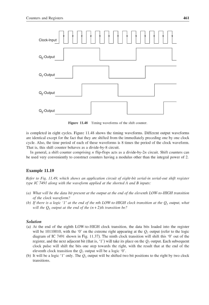
Figure 11.48 Timing waveforms of the shift counter.
is completed in eight cycles. Figure 11.48 shows the timing waveforms. Different output waveforms
are identical except for the fact that they are shifted from the immediately preceding one by one clock
cycle. Also, the time period of each of these waveforms is 8 times the period of the clock waveform.
That is, this shift counter behaves as a divide-by-8 circuit.
In general, a shift counter comprising n flip-flops acts as a divide-by-2n circuit. Shift counters can
be used very conveniently to construct counters having a modulus other than the integral power of 2.
Example 11.10
Refer to Fig. 11.49, which shows an application circuit of eight-bit serial-in serial-out shift register
type IC 7491 along with the waveform applied at the shorted A and B inputs:
(a) What will be the data bit present at the output at the end of the eleventh LOW-to-HIGH transition
of the clock waveform?
(b) If there is a logic ‘1’ at the end of the nth LOW-to-HIGH clock transition at the Q 3 output, what
will the Q 5 output at the end of the (n + 2)th transition be?
Solution
(a) At the end of the eighth LOW-to-HIGH clock transition, the data bits loaded into the register
will be 10110010, with the ‘0’ on the extreme right appearing at the Q 7 output (refer to the logic
diagram of IC 7491 shown in Fig. 11.37). The ninth clock transition will shift this ‘0’ out of the
register, and the next adjacent bit (that is, ‘1’) will take its place on the Q 7 output. Each subsequent
clock pulse will shift the bits one step towards the right, with the result that at the end of the
eleventh clock transition the Q 7 output will be a logic ‘0’.
(b) It will be a logic ‘1’ only. The Q 3 output will be shifted two bit positions to the right by two clock
transitions.
461
Clock-Input
Q -Output
0
Q -Output
1
Q -Output
2
Q -Output
3
Figure 11.48 Timing waveforms of the shift counter.
is completed in eight cycles. Figure 11.48 shows the timing waveforms. Different output waveforms
are identical except for the fact that they are shifted from the immediately preceding one by one clock
cycle. Also, the time period of each of these waveforms is 8 times the period of the clock waveform.
That is, this shift counter behaves as a divide-by-8 circuit.
In general, a shift counter comprising n flip-flops acts as a divide-by-2n circuit. Shift counters can
be used very conveniently to construct counters having a modulus other than the integral power of 2.
Example 11.10
Refer to Fig. 11.49, which shows an application circuit of eight-bit serial-in serial-out shift register
type IC 7491 along with the waveform applied at the shorted A and B inputs:
(a) What will be the data bit present at the output at the end of the eleventh LOW-to-HIGH transition
of the clock waveform?
(b) If there is a logic ‘1’ at the end of the nth LOW-to-HIGH clock transition at the Q 3 output, what
will the Q 5 output at the end of the (n + 2)th transition be?
Solution
(a) At the end of the eighth LOW-to-HIGH clock transition, the data bits loaded into the register
will be 10110010, with the ‘0’ on the extreme right appearing at the Q 7 output (refer to the logic
diagram of IC 7491 shown in Fig. 11.37). The ninth clock transition will shift this ‘0’ out of the
register, and the next adjacent bit (that is, ‘1’) will take its place on the Q 7 output. Each subsequent
clock pulse will shift the bits one step towards the right, with the result that at the end of the
eleventh clock transition the Q 7 output will be a logic ‘0’.
(b) It will be a logic ‘1’ only. The Q 3 output will be shifted two bit positions to the right by two clock
transitions.