

Counters and Registers
451
Table 11.14 Contents of four-bit serial-in serial-out shift register for the first eight clock cycles.
Clock
Q A
Q B
Q C
Q D
Initial contents
0
0
0
0
After first clock transition
1
0
0
0
After second clock transition
0
1
0
0
After third clock transition
0
0
1
0
After fourth clock transition
1
0
0
1
After fifth clock transition
0
1
0
0
After sixth clock transition
0
0
1
0
After seventh clock transition
0
0
0
1
After eighth clock transition
0
0
0
0
shown in Fig. 11.35, a data bit present at the data input terminal at the time of the nth clock transition
reaches the Q D output at the end of the (n + 4)th clock transition. During the fifth and subsequent
clock transitions, data bits continue to shift to the right, and at the end of the eighth clock transition
the shift register is again reset to all 0s. Thus, in a four-bit serial-in serial-out shift register, it takes
four clock cycles to load the data bits and another four cycles to read the data bits out of the register.
The contents of the register for the first eight clock cycles are summarized in Table 11.14. We can see
that the register is loaded with the four-bit data in four clock cycles, and also that the stored four-bit
data are read out in the subsequent four clock cycles.
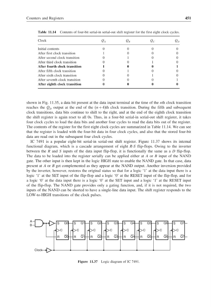
IC 7491 is a popular eight-bit serial-in serial-out shift register. Figure 11.37 shows its internal
functional diagram, which is a cascade arrangement of eight R-S flip-flops. Owing to the inverter
between the R and S inputs of the data input flip-flop, it is functionally the same as a D flip-flop.
The data to be loaded into the register serially can be applied either at A or B input of the NAND
gate. The other input is then kept in the logic HIGH state to enable the NAND gate. In that case, data
present at A or B get complemented as they appear at the NAND output. Another inversion provided
by the inverter, however, restores the original status so that for a logic ‘1’ at the data input there is a
logic ‘1’ at the SET input of the flip-flop and a logic ‘0’ at the RESET input of the flip-flop, and for
a logic ‘0’ at the data input there is a logic ‘0’ at the SET input and a logic ‘1’ at the RESET input
of the flip-flop. The NAND gate provides only a gating function, and, if it is not required, the two
inputs of the NAND can be shorted to have a single-line data input. The shift register responds to the
LOW-to-HIGH transitions of the clock pulses.
Q0
S
R
Q0
C
Q1
S
R
Q1
C
Q2
S
R
Q2
C
Q3
S
R
Q3
C
Q4
S
R
Q4
C
Q5
S
R
Q5
C
Q6
S
R
Q6
C
Q7
S
R
Q7
C
Clock
A
B
Figure 11.37 Logic diagram of IC 7491.
451
Table 11.14 Contents of four-bit serial-in serial-out shift register for the first eight clock cycles.
Clock
Q A
Q B
Q C
Q D
Initial contents
0
0
0
0
After first clock transition
1
0
0
0
After second clock transition
0
1
0
0
After third clock transition
0
0
1
0
After fourth clock transition
1
0
0
1
After fifth clock transition
0
1
0
0
After sixth clock transition
0
0
1
0
After seventh clock transition
0
0
0
1
After eighth clock transition
0
0
0
0
shown in Fig. 11.35, a data bit present at the data input terminal at the time of the nth clock transition
reaches the Q D output at the end of the (n + 4)th clock transition. During the fifth and subsequent
clock transitions, data bits continue to shift to the right, and at the end of the eighth clock transition
the shift register is again reset to all 0s. Thus, in a four-bit serial-in serial-out shift register, it takes
four clock cycles to load the data bits and another four cycles to read the data bits out of the register.
The contents of the register for the first eight clock cycles are summarized in Table 11.14. We can see
that the register is loaded with the four-bit data in four clock cycles, and also that the stored four-bit
data are read out in the subsequent four clock cycles.
IC 7491 is a popular eight-bit serial-in serial-out shift register. Figure 11.37 shows its internal
functional diagram, which is a cascade arrangement of eight R-S flip-flops. Owing to the inverter
between the R and S inputs of the data input flip-flop, it is functionally the same as a D flip-flop.
The data to be loaded into the register serially can be applied either at A or B input of the NAND
gate. The other input is then kept in the logic HIGH state to enable the NAND gate. In that case, data
present at A or B get complemented as they appear at the NAND output. Another inversion provided
by the inverter, however, restores the original status so that for a logic ‘1’ at the data input there is a
logic ‘1’ at the SET input of the flip-flop and a logic ‘0’ at the RESET input of the flip-flop, and for
a logic ‘0’ at the data input there is a logic ‘0’ at the SET input and a logic ‘1’ at the RESET input
of the flip-flop. The NAND gate provides only a gating function, and, if it is not required, the two
inputs of the NAND can be shorted to have a single-line data input. The shift register responds to the
LOW-to-HIGH transitions of the clock pulses.
Q0
S
R
Q0
C
Q1
S
R
Q1
C
Q2
S
R
Q2
C
Q3
S
R
Q3
C
Q4
S
R
Q4
C
Q5
S
R
Q5
C
Q6
S
R
Q6
C
Q7
S
R
Q7
C
Clock
A
B
Figure 11.37 Logic diagram of IC 7491.