

452
Digital Electronics
Q0
D
CD
CP
Q1
Q2
Q3
Q4
Q5
Q6
Q7
Clock
A
B
MR
D
CP
CD
D
CP
CD
D
CP
CD
D
CP
CD
D
CP
CD
D
CP
CD
Q7
Q6
Q5
Q4
D
CP
CD
Q3
Q2
Q1
Q0
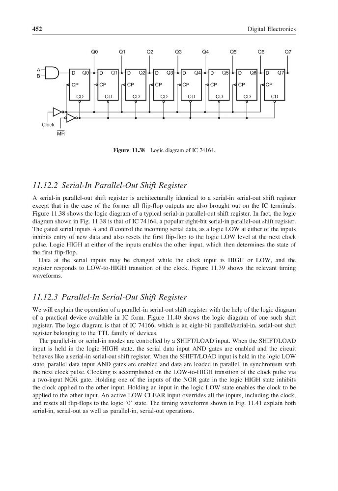
Figure 11.38 Logic diagram of IC 74164.
11.12.2 Serial-In Parallel-Out Shift Register
A serial-in parallel-out shift register is architecturally identical to a serial-in serial-out shift register
except that in the case of the former all flip-flop outputs are also brought out on the IC terminals.
Figure 11.38 shows the logic diagram of a typical serial-in parallel-out shift register. In fact, the logic
diagram shown in Fig. 11.38 is that of IC 74164, a popular eight-bit serial-in parallel-out shift register.
The gated serial inputs A and B control the incoming serial data, as a logic LOW at either of the inputs
inhibits entry of new data and also resets the first flip-flop to the logic LOW level at the next clock
pulse. Logic HIGH at either of the inputs enables the other input, which then determines the state of
the first flip-flop.
Data at the serial inputs may be changed while the clock input is HIGH or LOW, and the
register responds to LOW-to-HIGH transition of the clock. Figure 11.39 shows the relevant timing
waveforms.
11.12.3 Parallel-In Serial-Out Shift Register
We will explain the operation of a parallel-in serial-out shift register with the help of the logic diagram
of a practical device available in IC form. Figure 11.40 shows the logic diagram of one such shift
register. The logic diagram is that of IC 74166, which is an eight-bit parallel/serial-in, serial-out shift
register belonging to the TTL family of devices.
The parallel-in or serial-in modes are controlled by a SHIFT/LOAD input. When the SHIFT/LOAD
input is held in the logic HIGH state, the serial data input AND gates are enabled and the circuit
behaves like a serial-in serial-out shift register. When the SHIFT/LOAD input is held in the logic LOW
state, parallel data input AND gates are enabled and data are loaded in parallel, in synchronism with
the next clock pulse. Clocking is accomplished on the LOW-to-HIGH transition of the clock pulse via
a two-input NOR gate. Holding one of the inputs of the NOR gate in the logic HIGH state inhibits
the clock applied to the other input. Holding an input in the logic LOW state enables the clock to be
applied to the other input. An active LOW CLEAR input overrides all the inputs, including the clock,
and resets all flip-flops to the logic ‘0’ state. The timing waveforms shown in Fig. 11.41 explain both
serial-in, serial-out as well as parallel-in, serial-out operations.
Digital Electronics
Q0
D
CD
CP
Q1
Q2
Q3
Q4
Q5
Q6
Q7
Clock
A
B
MR
D
CP
CD
D
CP
CD
D
CP
CD
D
CP
CD
D
CP
CD
D
CP
CD
Q7
Q6
Q5
Q4
D
CP
CD
Q3
Q2
Q1
Q0
Figure 11.38 Logic diagram of IC 74164.
11.12.2 Serial-In Parallel-Out Shift Register
A serial-in parallel-out shift register is architecturally identical to a serial-in serial-out shift register
except that in the case of the former all flip-flop outputs are also brought out on the IC terminals.
Figure 11.38 shows the logic diagram of a typical serial-in parallel-out shift register. In fact, the logic
diagram shown in Fig. 11.38 is that of IC 74164, a popular eight-bit serial-in parallel-out shift register.
The gated serial inputs A and B control the incoming serial data, as a logic LOW at either of the inputs
inhibits entry of new data and also resets the first flip-flop to the logic LOW level at the next clock
pulse. Logic HIGH at either of the inputs enables the other input, which then determines the state of
the first flip-flop.
Data at the serial inputs may be changed while the clock input is HIGH or LOW, and the
register responds to LOW-to-HIGH transition of the clock. Figure 11.39 shows the relevant timing
waveforms.
11.12.3 Parallel-In Serial-Out Shift Register
We will explain the operation of a parallel-in serial-out shift register with the help of the logic diagram
of a practical device available in IC form. Figure 11.40 shows the logic diagram of one such shift
register. The logic diagram is that of IC 74166, which is an eight-bit parallel/serial-in, serial-out shift
register belonging to the TTL family of devices.
The parallel-in or serial-in modes are controlled by a SHIFT/LOAD input. When the SHIFT/LOAD
input is held in the logic HIGH state, the serial data input AND gates are enabled and the circuit
behaves like a serial-in serial-out shift register. When the SHIFT/LOAD input is held in the logic LOW
state, parallel data input AND gates are enabled and data are loaded in parallel, in synchronism with
the next clock pulse. Clocking is accomplished on the LOW-to-HIGH transition of the clock pulse via
a two-input NOR gate. Holding one of the inputs of the NOR gate in the logic HIGH state inhibits
the clock applied to the other input. Holding an input in the logic LOW state enables the clock to be
applied to the other input. An active LOW CLEAR input overrides all the inputs, including the clock,
and resets all flip-flops to the logic ‘0’ state. The timing waveforms shown in Fig. 11.41 explain both
serial-in, serial-out as well as parallel-in, serial-out operations.