

450
Digital Electronics
Q A
D
CL
Q B
D
CL
Q C
D
CL
Clk
Q D
D
CL
Data In
Clock
Clear
Data Out
Clk
Clk
Clk
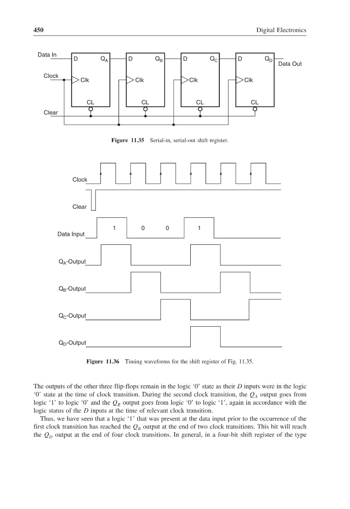
Figure 11.35 Serial-in, serial-out shift register.
Clock
Clear
Data Input
1
0
Q -Output
A
0
1
Q -Output
B
Q -Output
C
Q -Output
D
Figure 11.36 Timing waveforms for the shift register of Fig. 11.35.
The outputs of the other three flip-flops remain in the logic ‘0’ state as their D inputs were in the logic
‘0’ state at the time of clock transition. During the second clock transition, the Q A output goes from
logic ‘1’ to logic ‘0’ and the Q B output goes from logic ‘0’ to logic ‘1’, again in accordance with the
logic status of the D inputs at the time of relevant clock transition.
Thus, we have seen that a logic ‘1’ that was present at the data input prior to the occurrence of the
first clock transition has reached the Q B output at the end of two clock transitions. This bit will reach
the Q D output at the end of four clock transitions. In general, in a four-bit shift register of the type
Digital Electronics
Q A
D
CL
Q B
D
CL
Q C
D
CL
Clk
Q D
D
CL
Data In
Clock
Clear
Data Out
Clk
Clk
Clk
Figure 11.35 Serial-in, serial-out shift register.
Clock
Clear
Data Input
1
0
Q -Output
A
0
1
Q -Output
B
Q -Output
C
Q -Output
D
Figure 11.36 Timing waveforms for the shift register of Fig. 11.35.
The outputs of the other three flip-flops remain in the logic ‘0’ state as their D inputs were in the logic
‘0’ state at the time of clock transition. During the second clock transition, the Q A output goes from
logic ‘1’ to logic ‘0’ and the Q B output goes from logic ‘0’ to logic ‘1’, again in accordance with the
logic status of the D inputs at the time of relevant clock transition.
Thus, we have seen that a logic ‘1’ that was present at the data input prior to the occurrence of the
first clock transition has reached the Q B output at the end of two clock transitions. This bit will reach
the Q D output at the end of four clock transitions. In general, in a four-bit shift register of the type