

404
Digital Electronics
1
2
+V
+V
+V
0
Switch
Moved
from Pos-1
to Pos-2
Switch
Moved
from Pos-2
to Pos-1
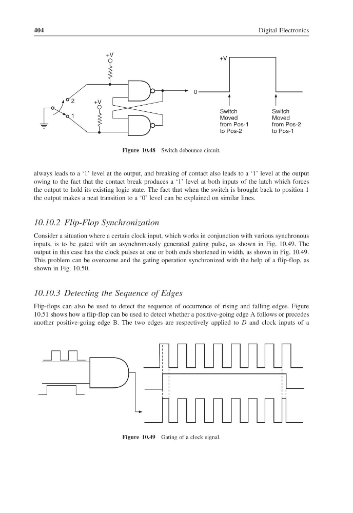
Figure 10.48 Switch debounce circuit.
always leads to a ‘1’ level at the output, and breaking of contact also leads to a ‘1’ level at the output
owing to the fact that the contact break produces a ‘1’ level at both inputs of the latch which forces
the output to hold its existing logic state. The fact that when the switch is brought back to position 1
the output makes a neat transition to a ‘0’ level can be explained on similar lines.
10.10.2 Flip-Flop Synchronization
Consider a situation where a certain clock input, which works in conjunction with various synchronous
inputs, is to be gated with an asynchronously generated gating pulse, as shown in Fig. 10.49. The
output in this case has the clock pulses at one or both ends shortened in width, as shown in Fig. 10.49.
This problem can be overcome and the gating operation synchronized with the help of a flip-flop, as
shown in Fig. 10.50.
10.10.3 Detecting the Sequence of Edges
Flip-flops can also be used to detect the sequence of occurrence of rising and falling edges. Figure
10.51 shows how a flip-flop can be used to detect whether a positive-going edge A follows or precedes
another positive-going edge B. The two edges are respectively applied to D and clock inputs of a
Figure 10.49 Gating of a clock signal.
Digital Electronics
1
2
+V
+V
+V
0
Switch
Moved
from Pos-1
to Pos-2
Switch
Moved
from Pos-2
to Pos-1
Figure 10.48 Switch debounce circuit.
always leads to a ‘1’ level at the output, and breaking of contact also leads to a ‘1’ level at the output
owing to the fact that the contact break produces a ‘1’ level at both inputs of the latch which forces
the output to hold its existing logic state. The fact that when the switch is brought back to position 1
the output makes a neat transition to a ‘0’ level can be explained on similar lines.
10.10.2 Flip-Flop Synchronization
Consider a situation where a certain clock input, which works in conjunction with various synchronous
inputs, is to be gated with an asynchronously generated gating pulse, as shown in Fig. 10.49. The
output in this case has the clock pulses at one or both ends shortened in width, as shown in Fig. 10.49.
This problem can be overcome and the gating operation synchronized with the help of a flip-flop, as
shown in Fig. 10.50.
10.10.3 Detecting the Sequence of Edges
Flip-flops can also be used to detect the sequence of occurrence of rising and falling edges. Figure
10.51 shows how a flip-flop can be used to detect whether a positive-going edge A follows or precedes
another positive-going edge B. The two edges are respectively applied to D and clock inputs of a
Figure 10.49 Gating of a clock signal.