

Flip-Flops and Related Devices
403
+V
2
1
(a)
+V
0
Bounce
(b)
(c)
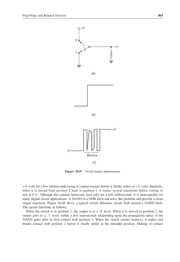
Figure 10.47 Switch bounce phenomenon.
+V volts for a few milliseconds owing to contact bounce before it finally settles at +V volts. Similarly,
when it is moved from position 2 back to position 1, it makes several transitions before coming to
rest at 0 V. Although this random behaviour lasts only for a few milliseconds, it is unacceptable for
many digital circuit applications. A NAND or a NOR latch can solve this problem and provide a clean
output transition. Figure 10.48 shows a typical switch debounce circuit built around a NAND latch.
The circuit functions as follows.
When the switch is in position 1, the output is at a ‘0’ level. When it is moved to position 2, the
output goes to a ‘1’ level within a few nanoseconds (depending upon the propagation delay of the
NAND gate) after its first contact with position 2. When the switch contact bounces, it makes and
breaks contact with position 2 before it finally settles at the intended position. Making of contact
403
+V
2
1
(a)
+V
0
Bounce
(b)
(c)
Figure 10.47 Switch bounce phenomenon.
+V volts for a few milliseconds owing to contact bounce before it finally settles at +V volts. Similarly,
when it is moved from position 2 back to position 1, it makes several transitions before coming to
rest at 0 V. Although this random behaviour lasts only for a few milliseconds, it is unacceptable for
many digital circuit applications. A NAND or a NOR latch can solve this problem and provide a clean
output transition. Figure 10.48 shows a typical switch debounce circuit built around a NAND latch.
The circuit functions as follows.
When the switch is in position 1, the output is at a ‘0’ level. When it is moved to position 2, the
output goes to a ‘1’ level within a few nanoseconds (depending upon the propagation delay of the
NAND gate) after its first contact with position 2. When the switch contact bounces, it makes and
breaks contact with position 2 before it finally settles at the intended position. Making of contact