

402
Digital Electronics
PRESET
————
CLEAR
———
or
t w
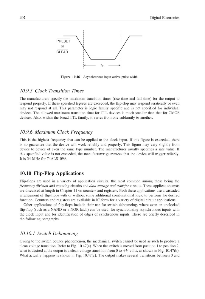
Figure 10.46 Asynchronous input active pulse width.
10.9.5 Clock Transition Times
The manufacturers specify the maximum transition times (rise time and fall time) for the output to
respond properly. If these specified figures are exceeded, the flip-flop may respond erratically or even
may not respond at all. This parameter is logic family specific and is not specified for individual
devices. The allowed maximum transition time for TTL devices is much smaller than that for CMOS
devices. Also, within the broad TTL family, it varies from one subfamily to another.
10.9.6 Maximum Clock Frequency
This is the highest frequency that can be applied to the clock input. If this figure is exceeded, there
is no guarantee that the device will work reliably and properly. This figure may vary slightly from
device to device of even the same type number. The manufacturer usually specifies a safe value. If
this specified value is not exceeded, the manufacturer guarantees that the device will trigger reliably.
It is 34 MHz for 74ALS109A.
10.10 Flip-Flop Applications
Flip-flops are used in a variety of application circuits, the most common among these being the
frequency division and counting circuits and data storage and transfer circuits. These application areas
are discussed at length in Chapter 11 on counters and registers. Both these applications use a cascaded
arrangement of flip-flops with or without some additional combinational logic to perform the desired
function. Counters and registers are available in IC form for a variety of digital circuit applications.
Other applications of flip-flops include their use for switch debouncing, where even an unclocked
flip-flop (such as a NAND or a NOR latch) can be used, for synchronizing asynchronous inputs with
the clock input and for identification of edges of synchronous inputs. These are briefly described in
the following paragraphs.
10.10.1 Switch Debouncing
Owing to the switch bounce phenomenon, the mechanical switch cannot be used as such to produce a
clean voltage transition. Refer to Fig. 10.47(a). When the switch is moved from position 1 to position 2,
what is desired at the output is a clean voltage transition from 0 to +V volts, as shown in Fig. 10.47(b).
What actually happens is shown in Fig. 10.47(c). The output makes several transitions between 0 and
Digital Electronics
PRESET
————
CLEAR
———
or
t w
Figure 10.46 Asynchronous input active pulse width.
10.9.5 Clock Transition Times
The manufacturers specify the maximum transition times (rise time and fall time) for the output to
respond properly. If these specified figures are exceeded, the flip-flop may respond erratically or even
may not respond at all. This parameter is logic family specific and is not specified for individual
devices. The allowed maximum transition time for TTL devices is much smaller than that for CMOS
devices. Also, within the broad TTL family, it varies from one subfamily to another.
10.9.6 Maximum Clock Frequency
This is the highest frequency that can be applied to the clock input. If this figure is exceeded, there
is no guarantee that the device will work reliably and properly. This figure may vary slightly from
device to device of even the same type number. The manufacturer usually specifies a safe value. If
this specified value is not exceeded, the manufacturer guarantees that the device will trigger reliably.
It is 34 MHz for 74ALS109A.
10.10 Flip-Flop Applications
Flip-flops are used in a variety of application circuits, the most common among these being the
frequency division and counting circuits and data storage and transfer circuits. These application areas
are discussed at length in Chapter 11 on counters and registers. Both these applications use a cascaded
arrangement of flip-flops with or without some additional combinational logic to perform the desired
function. Counters and registers are available in IC form for a variety of digital circuit applications.
Other applications of flip-flops include their use for switch debouncing, where even an unclocked
flip-flop (such as a NAND or a NOR latch) can be used, for synchronizing asynchronous inputs with
the clock input and for identification of edges of synchronous inputs. These are briefly described in
the following paragraphs.
10.10.1 Switch Debouncing
Owing to the switch bounce phenomenon, the mechanical switch cannot be used as such to produce a
clean voltage transition. Refer to Fig. 10.47(a). When the switch is moved from position 1 to position 2,
what is desired at the output is a clean voltage transition from 0 to +V volts, as shown in Fig. 10.47(b).
What actually happens is shown in Fig. 10.47(c). The output makes several transitions between 0 and