

Flip-Flops and Related Devices
405
Clock
D-Input
Q-Output
Output
Q
D
Clk
FF
Clock
Gating
Pulse
Output
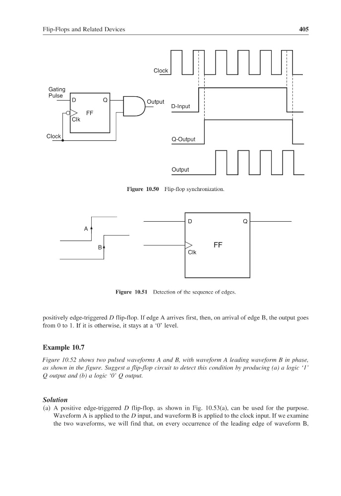
Figure 10.50 Flip-flop synchronization.
FF
Clk
D
Q
A
B
Figure 10.51 Detection of the sequence of edges.
positively edge-triggered D flip-flop. If edge A arrives first, then, on arrival of edge B, the output goes
from 0 to 1. If it is otherwise, it stays at a ‘0’ level.
Example 10.7
Figure 10.52 shows two pulsed waveforms A and B, with waveform A leading waveform B in phase,
as shown in the figure. Suggest a flip-flop circuit to detect this condition by producing (a) a logic ‘1’
Q output and (b) a logic ‘0’ Q output.
Solution
(a) A positive edge-triggered D flip-flop, as shown in Fig. 10.53(a), can be used for the purpose.
Waveform A is applied to the D input, and waveform B is applied to the clock input. If we examine
the two waveforms, we will find that, on every occurrence of the leading edge of waveform B,
405
Clock
D-Input
Q-Output
Output
Q
D
Clk
FF
Clock
Gating
Pulse
Output
Figure 10.50 Flip-flop synchronization.
FF
Clk
D
Q
A
B
Figure 10.51 Detection of the sequence of edges.
positively edge-triggered D flip-flop. If edge A arrives first, then, on arrival of edge B, the output goes
from 0 to 1. If it is otherwise, it stays at a ‘0’ level.
Example 10.7
Figure 10.52 shows two pulsed waveforms A and B, with waveform A leading waveform B in phase,
as shown in the figure. Suggest a flip-flop circuit to detect this condition by producing (a) a logic ‘1’
Q output and (b) a logic ‘0’ Q output.
Solution
(a) A positive edge-triggered D flip-flop, as shown in Fig. 10.53(a), can be used for the purpose.
Waveform A is applied to the D input, and waveform B is applied to the clock input. If we examine
the two waveforms, we will find that, on every occurrence of the leading edge of waveform B,