

376
Digital Electronics
S
Q
Q
R
S
R
Q
Operation
Mode
No change
SET
RESET
Forbidden
S
0
1
0
1
R
0
0
1
1
Q n+1
Q
1
0
—
n
(a)
(b)
(c)
RS
FF
Q
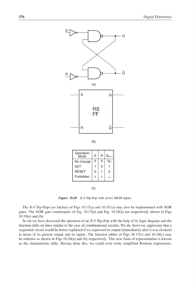
Figure 10.18 R-S flip-flop with active HIGH inputs.
The R-S flip-flops (or latches) of Figs 10.17(a) and 10.18 (a) may also be implemented with NOR
gates. The NOR gate counterparts of Fig. 10.17(a) and Fig. 10.18(a) are respectively shown in Figs
10.19(a) and (b).
So far we have discussed the operation of an R-S flip-flop with the help of its logic diagram and the
function table on lines similar to the case of combinational circuits. We do, however, appreciate that a
sequential circuit would be better explained if we expressed its output (immediately after it was clocked)
in terms of its present output and its inputs. The function tables of Figs 10.17(c) and 10.18(c) may
be redrawn as shown in Figs 10.20(a) and (b) respectively. This new form of representation is known
as the characteristic table. Having done this, we could even write simplified Boolean expressions,
Digital Electronics
S
Q
Q
R
S
R
Q
Operation
Mode
No change
SET
RESET
Forbidden
S
0
1
0
1
R
0
0
1
1
Q n+1
Q
1
0
—
n
(a)
(b)
(c)
RS
FF
Q
Figure 10.18 R-S flip-flop with active HIGH inputs.
The R-S flip-flops (or latches) of Figs 10.17(a) and 10.18 (a) may also be implemented with NOR
gates. The NOR gate counterparts of Fig. 10.17(a) and Fig. 10.18(a) are respectively shown in Figs
10.19(a) and (b).
So far we have discussed the operation of an R-S flip-flop with the help of its logic diagram and the
function table on lines similar to the case of combinational circuits. We do, however, appreciate that a
sequential circuit would be better explained if we expressed its output (immediately after it was clocked)
in terms of its present output and its inputs. The function tables of Figs 10.17(c) and 10.18(c) may
be redrawn as shown in Figs 10.20(a) and (b) respectively. This new form of representation is known
as the characteristic table. Having done this, we could even write simplified Boolean expressions,