

370
Digital Electronics
(a)
5
1
6, 7
555
4, 8
2
0.01
D
C
V CC
3
R
Trigger
I/p
v o
R 1
C 1
Trigger
I/P
At
pin-2
V CC
+0.7
V CC
0
0
(b)
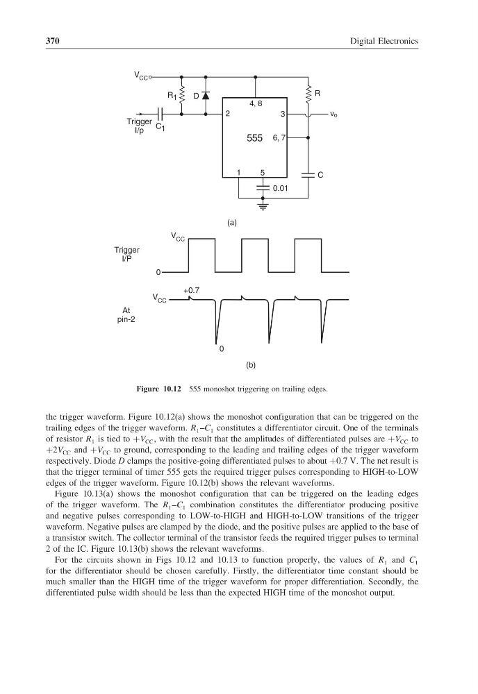
Figure 10.12 555 monoshot triggering on trailing edges.
the trigger waveform. Figure 10.12(a) shows the monoshot configuration that can be triggered on the
trailing edges of the trigger waveform. R 1 –C 1 constitutes a differentiator circuit. One of the terminals
of resistor R 1 is tied to +V CC , with the result that the amplitudes of differentiated pulses are +V CC to
+2V CC and +V CC to ground, corresponding to the leading and trailing edges of the trigger waveform
respectively. Diode D clamps the positive-going differentiated pulses to about +0.7 V. The net result is
that the trigger terminal of timer 555 gets the required trigger pulses corresponding to HIGH-to-LOW
edges of the trigger waveform. Figure 10.12(b) shows the relevant waveforms.
Figure 10.13(a) shows the monoshot configuration that can be triggered on the leading edges
of the trigger waveform. The R 1 –C 1 combination constitutes the differentiator producing positive
and negative pulses corresponding to LOW-to-HIGH and HIGH-to-LOW transitions of the trigger
waveform. Negative pulses are clamped by the diode, and the positive pulses are applied to the base of
a transistor switch. The collector terminal of the transistor feeds the required trigger pulses to terminal
2 of the IC. Figure 10.13(b) shows the relevant waveforms.
For the circuits shown in Figs 10.12 and 10.13 to function properly, the values of R 1 and C 1
for the differentiator should be chosen carefully. Firstly, the differentiator time constant should be
much smaller than the HIGH time of the trigger waveform for proper differentiation. Secondly, the
differentiated pulse width should be less than the expected HIGH time of the monoshot output.
Digital Electronics
(a)
5
1
6, 7
555
4, 8
2
0.01
D
C
V CC
3
R
Trigger
I/p
v o
R 1
C 1
Trigger
I/P
At
pin-2
V CC
+0.7
V CC
0
0
(b)
Figure 10.12 555 monoshot triggering on trailing edges.
the trigger waveform. Figure 10.12(a) shows the monoshot configuration that can be triggered on the
trailing edges of the trigger waveform. R 1 –C 1 constitutes a differentiator circuit. One of the terminals
of resistor R 1 is tied to +V CC , with the result that the amplitudes of differentiated pulses are +V CC to
+2V CC and +V CC to ground, corresponding to the leading and trailing edges of the trigger waveform
respectively. Diode D clamps the positive-going differentiated pulses to about +0.7 V. The net result is
that the trigger terminal of timer 555 gets the required trigger pulses corresponding to HIGH-to-LOW
edges of the trigger waveform. Figure 10.12(b) shows the relevant waveforms.
Figure 10.13(a) shows the monoshot configuration that can be triggered on the leading edges
of the trigger waveform. The R 1 –C 1 combination constitutes the differentiator producing positive
and negative pulses corresponding to LOW-to-HIGH and HIGH-to-LOW transitions of the trigger
waveform. Negative pulses are clamped by the diode, and the positive pulses are applied to the base of
a transistor switch. The collector terminal of the transistor feeds the required trigger pulses to terminal
2 of the IC. Figure 10.13(b) shows the relevant waveforms.
For the circuits shown in Figs 10.12 and 10.13 to function properly, the values of R 1 and C 1
for the differentiator should be chosen carefully. Firstly, the differentiator time constant should be
much smaller than the HIGH time of the trigger waveform for proper differentiation. Secondly, the
differentiated pulse width should be less than the expected HIGH time of the monoshot output.