

366
Digital Electronics
–
+
5K
–
+
5K
5K
V CC (Pin-8)
Reset (Pin-4)
Output (Pin-3)
Output
Stage
FF
Discharge
Transistor
Ground (Pin-1)
Control
(Pin-5)
Threshold
(Pin-6)
Trigger
(Pin-2)
Discharge
(Pin-7)
2
3
V CC
1
3
V CC
V ref (int)
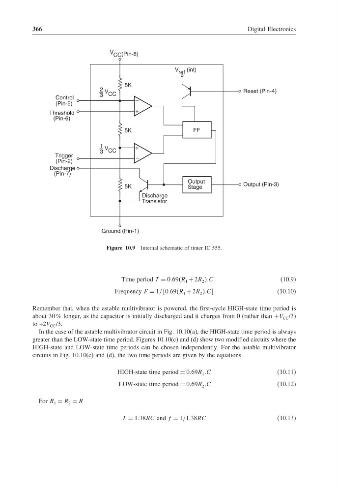
Figure 10.9 Internal schematic of timer IC 555.
Time period T = 069R 1 + 2R 2 C
(10.9)
Frequency F = 1/ 069R 1 + 2R 2 C
(10.10)
Remember that, when the astable multivibrator is powered, the first-cycle HIGH-state time period is
about 30 % longer, as the capacitor is initially discharged and it charges from 0 (rather than +V CC /3)
to +2V CC /3.
In the case of the astable multivibrator circuit in Fig. 10.10(a), the HIGH-state time period is always
greater than the LOW-state time period. Figures 10.10(c) and (d) show two modified circuits where the
HIGH-state and LOW-state time periods can be chosen independently. For the astable multivibrator
circuits in Fig. 10.10(c) and (d), the two time periods are given by the equations
HIGH-state time period = 069R 1 C
(10.11)
LOW-state time period = 069R 2 C
(10.12)
For R 1 = R 2 = R
T = 138RC and f = 1/138RC
(10.13)
Digital Electronics
–
+
5K
–
+
5K
5K
V CC (Pin-8)
Reset (Pin-4)
Output (Pin-3)
Output
Stage
FF
Discharge
Transistor
Ground (Pin-1)
Control
(Pin-5)
Threshold
(Pin-6)
Trigger
(Pin-2)
Discharge
(Pin-7)
2
3
V CC
1
3
V CC
V ref (int)
Figure 10.9 Internal schematic of timer IC 555.
Time period T = 069R 1 + 2R 2 C
(10.9)
Frequency F = 1/ 069R 1 + 2R 2 C
(10.10)
Remember that, when the astable multivibrator is powered, the first-cycle HIGH-state time period is
about 30 % longer, as the capacitor is initially discharged and it charges from 0 (rather than +V CC /3)
to +2V CC /3.
In the case of the astable multivibrator circuit in Fig. 10.10(a), the HIGH-state time period is always
greater than the LOW-state time period. Figures 10.10(c) and (d) show two modified circuits where the
HIGH-state and LOW-state time periods can be chosen independently. For the astable multivibrator
circuits in Fig. 10.10(c) and (d), the two time periods are given by the equations
HIGH-state time period = 069R 1 C
(10.11)
LOW-state time period = 069R 2 C
(10.12)
For R 1 = R 2 = R
T = 138RC and f = 1/138RC
(10.13)