

354
Digital Electronics
3. Determine the number of programmable interconnections in the following programmable logic
devices.
(a) 1K × 4 PROM;
(b) PLA device with four input variables, 32 AND gates and four OR gates;
(c) PAL device with eight input variables, 16 AND gates and four OR gates.
(a) 4096; (b) 384; (c) 256
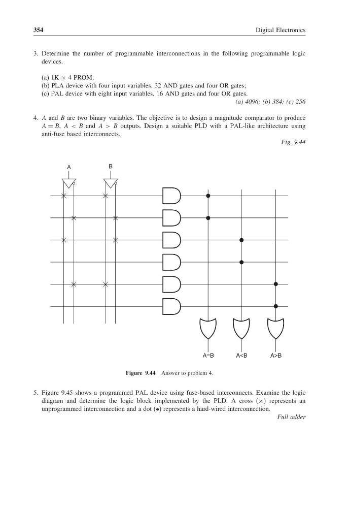
4. A and B are two binary variables. The objective is to design a magnitude comparator to produce
A = B, A < B and A > B outputs. Design a suitable PLD with a PAL-like architecture using
anti-fuse based interconnects.
Fig. 9.44
B
A
A=B
A
Figure 9.44 Answer to problem 4.
5. Figure 9.45 shows a programmed PAL device using fuse-based interconnects. Examine the logic
diagram and determine the logic block implemented by the PLD. A cross (× represents an
unprogrammed interconnection and a dot (•) represents a hard-wired interconnection.
Full adder
Digital Electronics
3. Determine the number of programmable interconnections in the following programmable logic
devices.
(a) 1K × 4 PROM;
(b) PLA device with four input variables, 32 AND gates and four OR gates;
(c) PAL device with eight input variables, 16 AND gates and four OR gates.
(a) 4096; (b) 384; (c) 256
4. A and B are two binary variables. The objective is to design a magnitude comparator to produce
A = B, A < B and A > B outputs. Design a suitable PLD with a PAL-like architecture using
anti-fuse based interconnects.
Fig. 9.44
B
A
A=B
A
Figure 9.44 Answer to problem 4.
5. Figure 9.45 shows a programmed PAL device using fuse-based interconnects. Examine the logic
diagram and determine the logic block implemented by the PLD. A cross (× represents an
unprogrammed interconnection and a dot (•) represents a hard-wired interconnection.
Full adder