

Programmable Logic Devices
353
6. What are the various interconnect technologies used for the purpose of programming PLDs? Briefly
describe each one of them.
7. What is a hardware description language? What are the requirements of a good HDL? Briefly
describe the salient features of VHDL and Verilog.
8. What do you understand by the following as regards programmable logic devices?
(a) combinational and registered outputs;
(b) configurable output logic cell;
(c) reprogrammable PLD;
(d) in-system programmability.
Problems
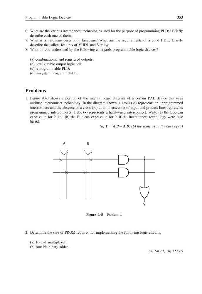
1. Figure 9.43 shows a portion of the internal logic diagram of a certain PAL device that uses
antifuse interconnect technology. In the diagram shown, a cross (× represents an unprogrammed
interconnect and the absence of a cross (× at an intersection of input and product lines represents
programmed interconnects; a dot (•) represents a hard-wired interconnect. Write (a) the Boolean
expression for Y and (b) the Boolean expression for Y if the interconnect technology were fuse
based.
(a) Y = AAB + AAB; (b) the same as in the case of (a)
B
A
Y
Figure 9.43 Problem 1.
2. Determine the size of PROM required for implementing the following logic circuits.
(a) 16-to-1 multiplexer;
(b) four-bit binary adder.
(a) 1M×1; (b) 512×5
353
6. What are the various interconnect technologies used for the purpose of programming PLDs? Briefly
describe each one of them.
7. What is a hardware description language? What are the requirements of a good HDL? Briefly
describe the salient features of VHDL and Verilog.
8. What do you understand by the following as regards programmable logic devices?
(a) combinational and registered outputs;
(b) configurable output logic cell;
(c) reprogrammable PLD;
(d) in-system programmability.
Problems
1. Figure 9.43 shows a portion of the internal logic diagram of a certain PAL device that uses
antifuse interconnect technology. In the diagram shown, a cross (× represents an unprogrammed
interconnect and the absence of a cross (× at an intersection of input and product lines represents
programmed interconnects; a dot (•) represents a hard-wired interconnect. Write (a) the Boolean
expression for Y and (b) the Boolean expression for Y if the interconnect technology were fuse
based.
(a) Y = AAB + AAB; (b) the same as in the case of (a)
B
A
Y
Figure 9.43 Problem 1.
2. Determine the size of PROM required for implementing the following logic circuits.
(a) 16-to-1 multiplexer;
(b) four-bit binary adder.
(a) 1M×1; (b) 512×5