

Programmable Logic Devices
337
Oxide
n+ diffusion
Poly-Si
Dielectric
(a)
Wire
Wire
Anti-fuse
(b)
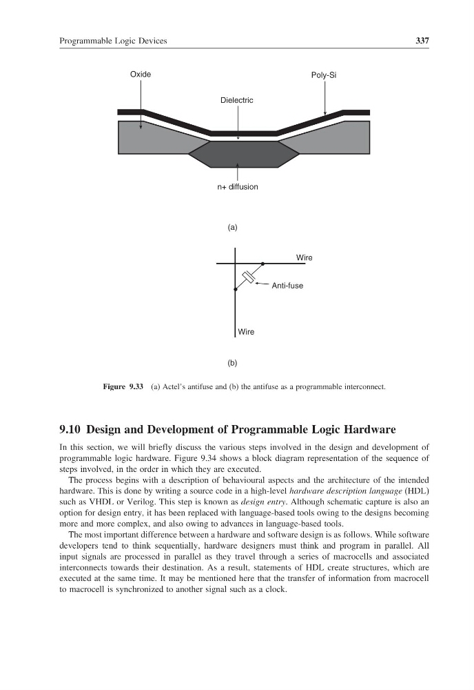
Figure 9.33 (a) Actel’s antifuse and (b) the antifuse as a programmable interconnect.
9.10 Design and Development of Programmable Logic Hardware
In this section, we will briefly discuss the various steps involved in the design and development of
programmable logic hardware. Figure 9.34 shows a block diagram representation of the sequence of
steps involved, in the order in which they are executed.
The process begins with a description of behavioural aspects and the architecture of the intended
hardware. This is done by writing a source code in a high-level hardware description language (HDL)
such as VHDL or Verilog. This step is known as design entry. Although schematic capture is also an
option for design entry, it has been replaced with language-based tools owing to the designs becoming
more and more complex, and also owing to advances in language-based tools.
The most important difference between a hardware and software design is as follows. While software
developers tend to think sequentially, hardware designers must think and program in parallel. All
input signals are processed in parallel as they travel through a series of macrocells and associated
interconnects towards their destination. As a result, statements of HDL create structures, which are
executed at the same time. It may be mentioned here that the transfer of information from macrocell
to macrocell is synchronized to another signal such as a clock.
337
Oxide
n+ diffusion
Poly-Si
Dielectric
(a)
Wire
Wire
Anti-fuse
(b)
Figure 9.33 (a) Actel’s antifuse and (b) the antifuse as a programmable interconnect.
9.10 Design and Development of Programmable Logic Hardware
In this section, we will briefly discuss the various steps involved in the design and development of
programmable logic hardware. Figure 9.34 shows a block diagram representation of the sequence of
steps involved, in the order in which they are executed.
The process begins with a description of behavioural aspects and the architecture of the intended
hardware. This is done by writing a source code in a high-level hardware description language (HDL)
such as VHDL or Verilog. This step is known as design entry. Although schematic capture is also an
option for design entry, it has been replaced with language-based tools owing to the designs becoming
more and more complex, and also owing to advances in language-based tools.
The most important difference between a hardware and software design is as follows. While software
developers tend to think sequentially, hardware designers must think and program in parallel. All
input signals are processed in parallel as they travel through a series of macrocells and associated
interconnects towards their destination. As a result, statements of HDL create structures, which are
executed at the same time. It may be mentioned here that the transfer of information from macrocell
to macrocell is synchronized to another signal such as a clock.