

336
Digital Electronics
SRAM
SRAM
SRAM
Logic Cell
Logic Cell
Logic Cell
Logic Cell
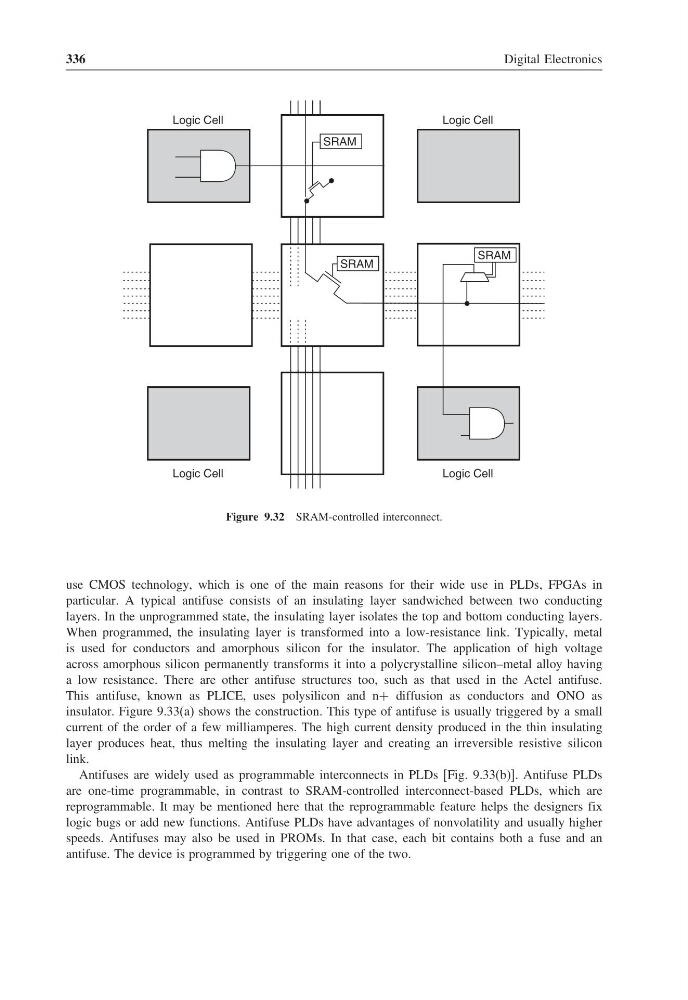
Figure 9.32 SRAM-controlled interconnect.
use CMOS technology, which is one of the main reasons for their wide use in PLDs, FPGAs in
particular. A typical antifuse consists of an insulating layer sandwiched between two conducting
layers. In the unprogrammed state, the insulating layer isolates the top and bottom conducting layers.
When programmed, the insulating layer is transformed into a low-resistance link. Typically, metal
is used for conductors and amorphous silicon for the insulator. The application of high voltage
across amorphous silicon permanently transforms it into a polycrystalline silicon–metal alloy having
a low resistance. There are other antifuse structures too, such as that used in the Actel antifuse.
This antifuse, known as PLICE, uses polysilicon and n+ diffusion as conductors and ONO as
insulator. Figure 9.33(a) shows the construction. This type of antifuse is usually triggered by a small
current of the order of a few milliamperes. The high current density produced in the thin insulating
layer produces heat, thus melting the insulating layer and creating an irreversible resistive silicon
link.
Antifuses are widely used as programmable interconnects in PLDs [Fig. 9.33(b)]. Antifuse PLDs
are one-time programmable, in contrast to SRAM-controlled interconnect-based PLDs, which are
reprogrammable. It may be mentioned here that the reprogrammable feature helps the designers fix
logic bugs or add new functions. Antifuse PLDs have advantages of nonvolatility and usually higher
speeds. Antifuses may also be used in PROMs. In that case, each bit contains both a fuse and an
antifuse. The device is programmed by triggering one of the two.
Digital Electronics
SRAM
SRAM
SRAM
Logic Cell
Logic Cell
Logic Cell
Logic Cell
Figure 9.32 SRAM-controlled interconnect.
use CMOS technology, which is one of the main reasons for their wide use in PLDs, FPGAs in
particular. A typical antifuse consists of an insulating layer sandwiched between two conducting
layers. In the unprogrammed state, the insulating layer isolates the top and bottom conducting layers.
When programmed, the insulating layer is transformed into a low-resistance link. Typically, metal
is used for conductors and amorphous silicon for the insulator. The application of high voltage
across amorphous silicon permanently transforms it into a polycrystalline silicon–metal alloy having
a low resistance. There are other antifuse structures too, such as that used in the Actel antifuse.
This antifuse, known as PLICE, uses polysilicon and n+ diffusion as conductors and ONO as
insulator. Figure 9.33(a) shows the construction. This type of antifuse is usually triggered by a small
current of the order of a few milliamperes. The high current density produced in the thin insulating
layer produces heat, thus melting the insulating layer and creating an irreversible resistive silicon
link.
Antifuses are widely used as programmable interconnects in PLDs [Fig. 9.33(b)]. Antifuse PLDs
are one-time programmable, in contrast to SRAM-controlled interconnect-based PLDs, which are
reprogrammable. It may be mentioned here that the reprogrammable feature helps the designers fix
logic bugs or add new functions. Antifuse PLDs have advantages of nonvolatility and usually higher
speeds. Antifuses may also be used in PROMs. In that case, each bit contains both a fuse and an
antifuse. The device is programmed by triggering one of the two.