

Programmable Logic Devices
335
The use of multiplexers can reduce this number significantly and can also address the problem of
increased propagation delay. An MUX-based interconnect matrix is being used in CPLDs. CPLD type
XPLA3 from Xilinx is an example.
9.9.3 Static RAM-Controlled Programmable Switches
Static RAM (SRAM) is basically a semiconductor memory, and the word ‘static’ implies that it is a
nonvolatile memory. That is, the memory retains its contents as long as power is on. A SRAM with
m address lines and n data lines is referred to as a 2
m
× n memory and is capable of storing 2
m n-bit
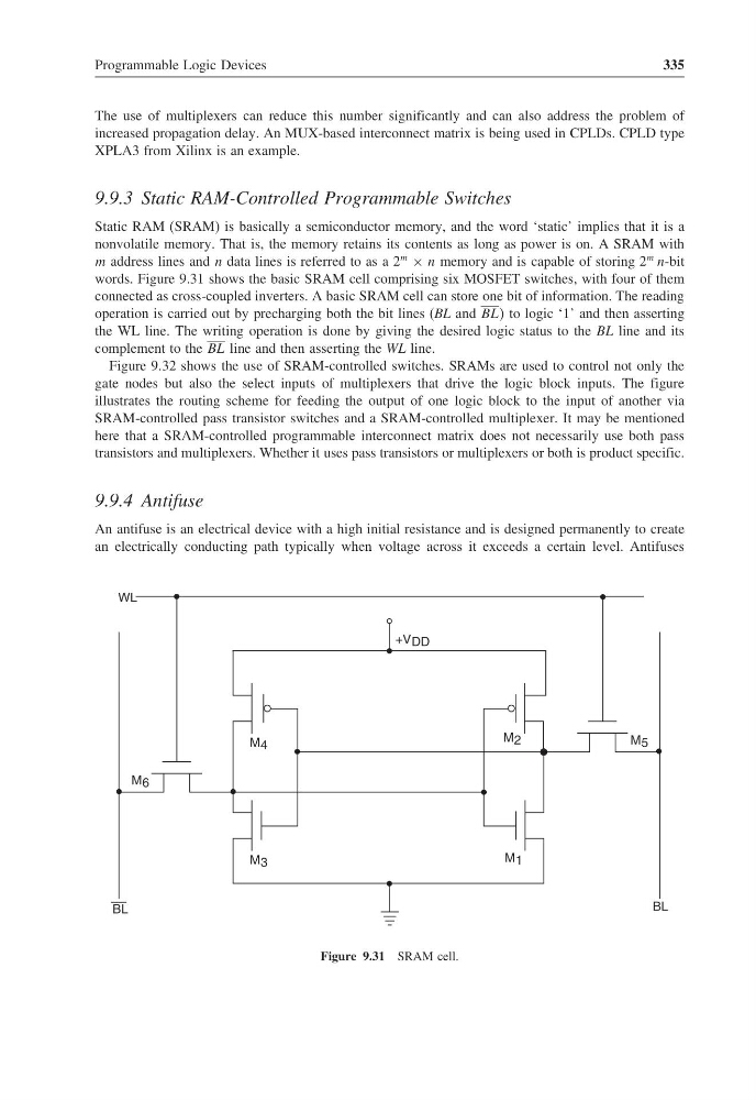
words. Figure 9.31 shows the basic SRAM cell comprising six MOSFET switches, with four of them
connected as cross-coupled inverters. A basic SRAM cell can store one bit of information. The reading
operation is carried out by precharging both the bit lines (BL and BLL to logic ‘1’ and then asserting
the WL line. The writing operation is done by giving the desired logic status to the BL line and its
complement to the BL line and then asserting the WL line.
Figure 9.32 shows the use of SRAM-controlled switches. SRAMs are used to control not only the
gate nodes but also the select inputs of multiplexers that drive the logic block inputs. The figure
illustrates the routing scheme for feeding the output of one logic block to the input of another via
SRAM-controlled pass transistor switches and a SRAM-controlled multiplexer. It may be mentioned
here that a SRAM-controlled programmable interconnect matrix does not necessarily use both pass
transistors and multiplexers. Whether it uses pass transistors or multiplexers or both is product specific.
9.9.4 Antifuse
An antifuse is an electrical device with a high initial resistance and is designed permanently to create
an electrically conducting path typically when voltage across it exceeds a certain level. Antifuses
M 3
M 4
M 6
M 2
M 1
M 5
WL
+V DD
BL
BL
Figure 9.31 SRAM cell.
335
The use of multiplexers can reduce this number significantly and can also address the problem of
increased propagation delay. An MUX-based interconnect matrix is being used in CPLDs. CPLD type
XPLA3 from Xilinx is an example.
9.9.3 Static RAM-Controlled Programmable Switches
Static RAM (SRAM) is basically a semiconductor memory, and the word ‘static’ implies that it is a
nonvolatile memory. That is, the memory retains its contents as long as power is on. A SRAM with
m address lines and n data lines is referred to as a 2
m
× n memory and is capable of storing 2
m n-bit
words. Figure 9.31 shows the basic SRAM cell comprising six MOSFET switches, with four of them
connected as cross-coupled inverters. A basic SRAM cell can store one bit of information. The reading
operation is carried out by precharging both the bit lines (BL and BLL to logic ‘1’ and then asserting
the WL line. The writing operation is done by giving the desired logic status to the BL line and its
complement to the BL line and then asserting the WL line.
Figure 9.32 shows the use of SRAM-controlled switches. SRAMs are used to control not only the
gate nodes but also the select inputs of multiplexers that drive the logic block inputs. The figure
illustrates the routing scheme for feeding the output of one logic block to the input of another via
SRAM-controlled pass transistor switches and a SRAM-controlled multiplexer. It may be mentioned
here that a SRAM-controlled programmable interconnect matrix does not necessarily use both pass
transistors and multiplexers. Whether it uses pass transistors or multiplexers or both is product specific.
9.9.4 Antifuse
An antifuse is an electrical device with a high initial resistance and is designed permanently to create
an electrically conducting path typically when voltage across it exceeds a certain level. Antifuses
M 3
M 4
M 6
M 2
M 1
M 5
WL
+V DD
BL
BL
Figure 9.31 SRAM cell.