

332
Digital Electronics
FF
Q
clk
Clock
D
O/P
4-input
LUT
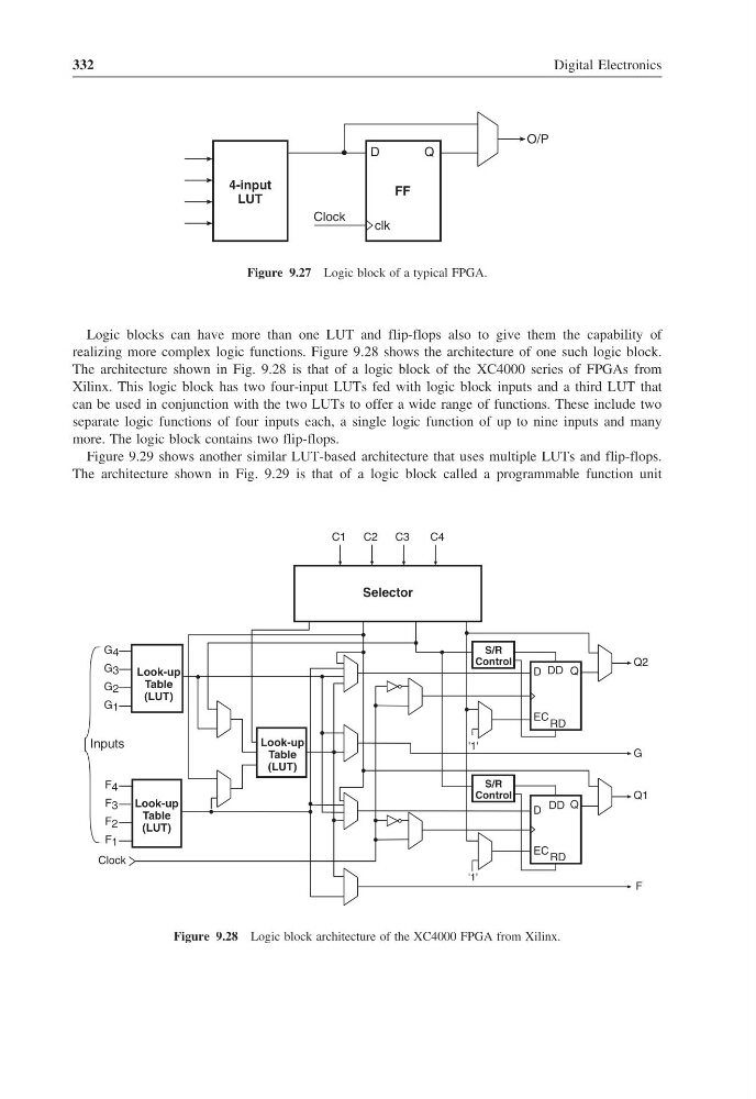
Figure 9.27 Logic block of a typical FPGA.
Logic blocks can have more than one LUT and flip-flops also to give them the capability of
realizing more complex logic functions. Figure 9.28 shows the architecture of one such logic block.
The architecture shown in Fig. 9.28 is that of a logic block of the XC4000 series of FPGAs from
Xilinx. This logic block has two four-input LUTs fed with logic block inputs and a third LUT that
can be used in conjunction with the two LUTs to offer a wide range of functions. These include two
separate logic functions of four inputs each, a single logic function of up to nine inputs and many
more. The logic block contains two flip-flops.
Figure 9.29 shows another similar LUT-based architecture that uses multiple LUTs and flip-flops.
The architecture shown in Fig. 9.29 is that of a logic block called a programmable function unit
DD
RD
EC
Q
D
S/R
Control
DD
RD
EC
Q
D
S/R
Control
Look-up
Table
(LUT)
Look-up
Table
(LUT)
Look-up
Table
(LUT)
Selector
G 2
G 1
F 4
F 3
F 2
C1
C2
C3
C4
Q2
G
Q1
F
Clock
'1'
'1'
G 4
G 3
F 1
Inputs
Figure 9.28 Logic block architecture of the XC4000 FPGA from Xilinx.
Digital Electronics
FF
Q
clk
Clock
D
O/P
4-input
LUT
Figure 9.27 Logic block of a typical FPGA.
Logic blocks can have more than one LUT and flip-flops also to give them the capability of
realizing more complex logic functions. Figure 9.28 shows the architecture of one such logic block.
The architecture shown in Fig. 9.28 is that of a logic block of the XC4000 series of FPGAs from
Xilinx. This logic block has two four-input LUTs fed with logic block inputs and a third LUT that
can be used in conjunction with the two LUTs to offer a wide range of functions. These include two
separate logic functions of four inputs each, a single logic function of up to nine inputs and many
more. The logic block contains two flip-flops.
Figure 9.29 shows another similar LUT-based architecture that uses multiple LUTs and flip-flops.
The architecture shown in Fig. 9.29 is that of a logic block called a programmable function unit
DD
RD
EC
Q
D
S/R
Control
DD
RD
EC
Q
D
S/R
Control
Look-up
Table
(LUT)
Look-up
Table
(LUT)
Look-up
Table
(LUT)
Selector
G 2
G 1
F 4
F 3
F 2
C1
C2
C3
C4
Q2
G
Q1
F
Clock
'1'
'1'
G 4
G 3
F 1
Inputs
Figure 9.28 Logic block architecture of the XC4000 FPGA from Xilinx.