

Programmable Logic Devices
333
D FF Q
D FF Q
LUT
LUT
LUT
LUT
Switch
Maxtrix
Inputs
D FF Q
D FF Q
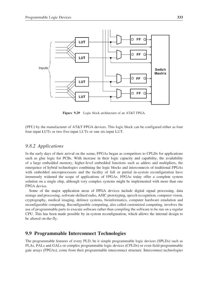
Figure 9.29 Logic block architecture of an AT&T FPGA.
(PFU) by the manufacturer of AT&T FPGA devices. This logic block can be configured either as four
four-input LUTs or two five-input LUTs or one six-input LUT.
9.8.2 Applications
In the early days of their arrival on the scene, FPGAs began as competitors to CPLDs for applications
such as glue logic for PCBs. With increase in their logic capacity and capability, the availability
of a large embedded memory, higher-level embedded functions such as adders and multipliers, the
emergence of hybrid technologies combining the logic blocks and interconnects of traditional FPGAs
with embedded microprocessors and the facility of full or partial in-system reconfiguration have
immensely widened the scope of applications of FPGAs. FPGAs today offer a complete system
solution on a single chip, although very complex systems might be implemented with more than one
FPGA device.
Some of the major application areas of FPGA devices include digital signal processing, data
storage and processing, software-defined radio, ASIC prototyping, speech recognition, computer vision,
cryptography, medical imaging, defence systems, bioinformatics, computer hardware emulation and
reconfigurable computing. Reconfigurable computing, also called customized computing, involves the
use of programmable parts to execute software rather than compiling the software to be run on a regular
CPU. This has been made possible by in-system reconfiguration, which allows the internal design to
be altered on-the-fly.
9.9 Programmable Interconnect Technologies
The programmable features of every PLD, be it simple programmable logic devices (SPLDs) such as
PLAs, PALs and GALs or complex programmable logic devices (CPLDs) or even field-programmable
gate arrays (FPGAs), come from their programmable interconnect structure. Interconnect technologies
333
D FF Q
D FF Q
LUT
LUT
LUT
LUT
Switch
Maxtrix
Inputs
D FF Q
D FF Q
Figure 9.29 Logic block architecture of an AT&T FPGA.
(PFU) by the manufacturer of AT&T FPGA devices. This logic block can be configured either as four
four-input LUTs or two five-input LUTs or one six-input LUT.
9.8.2 Applications
In the early days of their arrival on the scene, FPGAs began as competitors to CPLDs for applications
such as glue logic for PCBs. With increase in their logic capacity and capability, the availability
of a large embedded memory, higher-level embedded functions such as adders and multipliers, the
emergence of hybrid technologies combining the logic blocks and interconnects of traditional FPGAs
with embedded microprocessors and the facility of full or partial in-system reconfiguration have
immensely widened the scope of applications of FPGAs. FPGAs today offer a complete system
solution on a single chip, although very complex systems might be implemented with more than one
FPGA device.
Some of the major application areas of FPGA devices include digital signal processing, data
storage and processing, software-defined radio, ASIC prototyping, speech recognition, computer vision,
cryptography, medical imaging, defence systems, bioinformatics, computer hardware emulation and
reconfigurable computing. Reconfigurable computing, also called customized computing, involves the
use of programmable parts to execute software rather than compiling the software to be run on a regular
CPU. This has been made possible by in-system reconfiguration, which allows the internal design to
be altered on-the-fly.
9.9 Programmable Interconnect Technologies
The programmable features of every PLD, be it simple programmable logic devices (SPLDs) such as
PLAs, PALs and GALs or complex programmable logic devices (CPLDs) or even field-programmable
gate arrays (FPGAs), come from their programmable interconnect structure. Interconnect technologies