

Programmable Logic Devices
313
A
B
C
D
Programmable OR-array
Y1
Y2
Y3
Y4
Programmable AND-array
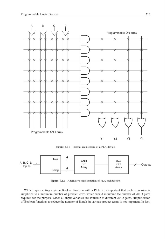
Figure 9.11 Internal architecture of a PLA device.
True
Comp.
Outputs
AND
8x8
Array
8x4
OR
Array
4
4
A, B, C, D
Inputs
Figure 9.12 Alternative representation of PLA architecture.
While implementing a given Boolean function with a PLA, it is important that each expression is
simplified to a minimum number of product terms which would minimize the number of AND gates
required for the purpose. Since all input variables are available to different AND gates, simplification
of Boolean functions to reduce the number of literals in various product terms is not important. In fact,
313
A
B
C
D
Programmable OR-array
Y1
Y2
Y3
Y4
Programmable AND-array
Figure 9.11 Internal architecture of a PLA device.
True
Comp.
Outputs
AND
8x8
Array
8x4
OR
Array
4
4
A, B, C, D
Inputs
Figure 9.12 Alternative representation of PLA architecture.
While implementing a given Boolean function with a PLA, it is important that each expression is
simplified to a minimum number of product terms which would minimize the number of AND gates
required for the purpose. Since all input variables are available to different AND gates, simplification
of Boolean functions to reduce the number of literals in various product terms is not important. In fact,