

Multiplexers and Demultiplexers
271
16-to-1
MUX
G
A
B
C
D
D0
D1
D2
D3
D4
D5
D6
D7
D8
D9
D10
D11
D12
D13
D14
D15
W
X
L
L
L
L
L
L
L
L
H
H
H
H
H
H
H
H
X
L
L
L
L
H
H
H
H
L
L
L
L
H
H
H
H
X
L
L
H
H
L
L
H
H
L
L
H
H
L
L
H
H
X
L
H
L
H
L
H
L
H
L
H
L
H
L
H
L
H
H
L
L
L
L
L
L
L
L
L
L
L
L
L
L
L
L
H
D0
D1
D2
D3
D4
D5
D6
D7
D8
D9
D10
D11
D12
D13
D14
D15
Output
W
Enable
G
Select
D
C
B A
Inputs
(a)
(b)
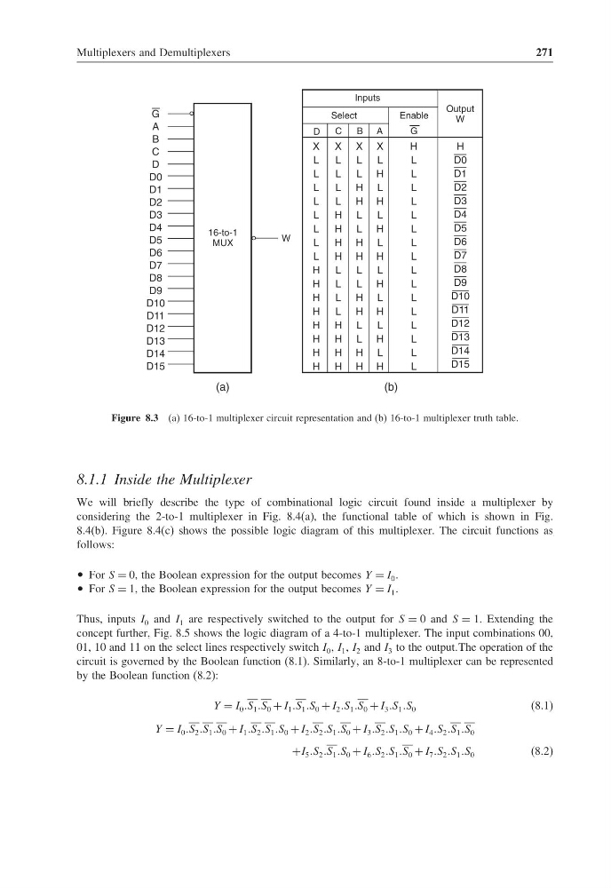
Figure 8.3 (a) 16-to-1 multiplexer circuit representation and (b) 16-to-1 multiplexer truth table.
8.1.1 Inside the Multiplexer
We will briefly describe the type of combinational logic circuit found inside a multiplexer by
considering the 2-to-1 multiplexer in Fig. 8.4(a), the functional table of which is shown in Fig.
8.4(b). Figure 8.4(c) shows the possible logic diagram of this multiplexer. The circuit functions as
follows:
• For S = 0, the Boolean expression for the output becomes Y = I 0 .
• For S = 1, the Boolean expression for the output becomes Y = I 1 .
Thus, inputs I 0 and I 1 are respectively switched to the output for S = 0 and S = 1. Extending the
concept further, Fig. 8.5 shows the logic diagram of a 4-to-1 multiplexer. The input combinations 00,
01, 10 and 11 on the select lines respectively switch I 0 , I 1 , I 2 and I 3 to the output.The operation of the
circuit is governed by the Boolean function (8.1). Similarly, an 8-to-1 multiplexer can be represented
by the Boolean function (8.2):
Y = I 0 S 1 S 0 + I 1 S 1 S 0 + I 2 S 1 S 0 + I 3 S 1 S 0
(8.1)
Y = I 0 S 2 S 1 S 0 + I 1 S 2 S 1 S 0 + I 2 S 2 S 1 S 0 + I 3 S 2 S 1 S 0 + I 4 S 2 S 1 S 0
+I 5 S 2 S 1 S 0 + I 6 S 2 S 1 S 0 + I 7 S 2 S 1 S 0
(8.2)
271
16-to-1
MUX
G
A
B
C
D
D0
D1
D2
D3
D4
D5
D6
D7
D8
D9
D10
D11
D12
D13
D14
D15
W
X
L
L
L
L
L
L
L
L
H
H
H
H
H
H
H
H
X
L
L
L
L
H
H
H
H
L
L
L
L
H
H
H
H
X
L
L
H
H
L
L
H
H
L
L
H
H
L
L
H
H
X
L
H
L
H
L
H
L
H
L
H
L
H
L
H
L
H
H
L
L
L
L
L
L
L
L
L
L
L
L
L
L
L
L
H
D0
D1
D2
D3
D4
D5
D6
D7
D8
D9
D10
D11
D12
D13
D14
D15
Output
W
Enable
G
Select
D
C
B A
Inputs
(a)
(b)
Figure 8.3 (a) 16-to-1 multiplexer circuit representation and (b) 16-to-1 multiplexer truth table.
8.1.1 Inside the Multiplexer
We will briefly describe the type of combinational logic circuit found inside a multiplexer by
considering the 2-to-1 multiplexer in Fig. 8.4(a), the functional table of which is shown in Fig.
8.4(b). Figure 8.4(c) shows the possible logic diagram of this multiplexer. The circuit functions as
follows:
• For S = 0, the Boolean expression for the output becomes Y = I 0 .
• For S = 1, the Boolean expression for the output becomes Y = I 1 .
Thus, inputs I 0 and I 1 are respectively switched to the output for S = 0 and S = 1. Extending the
concept further, Fig. 8.5 shows the logic diagram of a 4-to-1 multiplexer. The input combinations 00,
01, 10 and 11 on the select lines respectively switch I 0 , I 1 , I 2 and I 3 to the output.The operation of the
circuit is governed by the Boolean function (8.1). Similarly, an 8-to-1 multiplexer can be represented
by the Boolean function (8.2):
Y = I 0 S 1 S 0 + I 1 S 1 S 0 + I 2 S 1 S 0 + I 3 S 1 S 0
(8.1)
Y = I 0 S 2 S 1 S 0 + I 1 S 2 S 1 S 0 + I 2 S 2 S 1 S 0 + I 3 S 2 S 1 S 0 + I 4 S 2 S 1 S 0
+I 5 S 2 S 1 S 0 + I 6 S 2 S 1 S 0 + I 7 S 2 S 1 S 0
(8.2)