

254
Digital Electronics
Output
Carry
S 7
B 7 B 6 B 5 B 4
A 7 A 6 A 5 A 4
7483
(4-BitBinaryAdder)
7483
(4-BitBinaryAdder)
Z 7 Z 6 Z 5 Z 4
S 6 S 5 S 4
S 3
B 3 B 2 B 1 B 0 A 3 A 2 A 1 A 0
Z 3 Z 2 Z 1 Z 0
S 2 S 1 S 0
Carry In
7483
(4-BitBinaryAdder)
7483
(4-BitBinaryAdder)
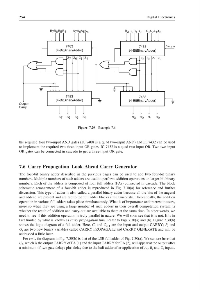
Figure 7.29 Example 7.6.
the required four two-input AND gates (IC 7408 is a quad two-input AND) and IC 7432 can be used
to implement the required two three-input OR gates. IC 7432 is a quad two-input OR. Two two-input
OR gates can be connected in cascade to get a three-input OR gate.
7.6 Carry Propagation–Look-Ahead Carry Generator
The four-bit binary adder described in the previous pages can be used to add two four-bit binary
numbers. Multiple numbers of such adders are used to perform addition operations on larger-bit binary
numbers. Each of the adders is composed of four full adders (FAs) connected in cascade. The block
schematic arrangement of a four-bit adder is reproduced in Fig. 7.30(a) for reference and further
discussion. This type of adder is also called a parallel binary adder because all the bits of the augend
and addend are present and are fed to the full adder blocks simultaneously. Theoretically, the addition
operation in various full adders takes place simultaneously. What is of importance and interest to users,
more so when they are using a large number of such adders in their overall computation system, is
whether the result of addition and carry-out are available to them at the same time. In other words, we
need to see if this addition operation is truly parallel in nature. We will soon see that it is not. It is in
fact limited by what is known as carry propagation time. Refer to Figs 7.30(a) and (b). Figure 7.30(b)
shows the logic diagram of a full adder. Here, C i and C i+1 are the input and output CARRY; P i and
G i are two new binary variables called CARRY PROPAGATE and CARRY GENERATE and will be
addressed a little later.
For i=1, the diagram in Fig. 7.30(b) is that of the LSB full adder of Fig. 7.30(a). We can see here that
C 2 , which is the output CARRY of FA (1) and the input CARRY for FA (2), will appear at the output after
a minimum of two gate delays plus delay due to the half adder after application of A i , B i and C i inputs.
Digital Electronics
Output
Carry
S 7
B 7 B 6 B 5 B 4
A 7 A 6 A 5 A 4
7483
(4-BitBinaryAdder)
7483
(4-BitBinaryAdder)
Z 7 Z 6 Z 5 Z 4
S 6 S 5 S 4
S 3
B 3 B 2 B 1 B 0 A 3 A 2 A 1 A 0
Z 3 Z 2 Z 1 Z 0
S 2 S 1 S 0
Carry In
7483
(4-BitBinaryAdder)
7483
(4-BitBinaryAdder)
Figure 7.29 Example 7.6.
the required four two-input AND gates (IC 7408 is a quad two-input AND) and IC 7432 can be used
to implement the required two three-input OR gates. IC 7432 is a quad two-input OR. Two two-input
OR gates can be connected in cascade to get a three-input OR gate.
7.6 Carry Propagation–Look-Ahead Carry Generator
The four-bit binary adder described in the previous pages can be used to add two four-bit binary
numbers. Multiple numbers of such adders are used to perform addition operations on larger-bit binary
numbers. Each of the adders is composed of four full adders (FAs) connected in cascade. The block
schematic arrangement of a four-bit adder is reproduced in Fig. 7.30(a) for reference and further
discussion. This type of adder is also called a parallel binary adder because all the bits of the augend
and addend are present and are fed to the full adder blocks simultaneously. Theoretically, the addition
operation in various full adders takes place simultaneously. What is of importance and interest to users,
more so when they are using a large number of such adders in their overall computation system, is
whether the result of addition and carry-out are available to them at the same time. In other words, we
need to see if this addition operation is truly parallel in nature. We will soon see that it is not. It is in
fact limited by what is known as carry propagation time. Refer to Figs 7.30(a) and (b). Figure 7.30(b)
shows the logic diagram of a full adder. Here, C i and C i+1 are the input and output CARRY; P i and
G i are two new binary variables called CARRY PROPAGATE and CARRY GENERATE and will be
addressed a little later.
For i=1, the diagram in Fig. 7.30(b) is that of the LSB full adder of Fig. 7.30(a). We can see here that
C 2 , which is the output CARRY of FA (1) and the input CARRY for FA (2), will appear at the output after
a minimum of two gate delays plus delay due to the half adder after application of A i , B i and C i inputs.