

Arithmetic Circuits
237
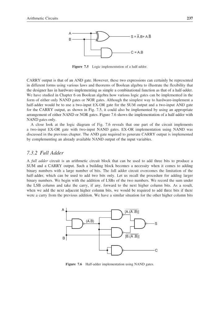
Figure 7.5 Logic implementation of a half-adder.
CARRY output is that of an AND gate. However, these two expressions can certainly be represented
in different forms using various laws and theorems of Boolean algebra to illustrate the flexibility that
the designer has in hardware-implementing as simple a combinational function as that of a half-adder.
We have studied in Chapter 6 on Boolean algebra how various logic gates can be implemented in the
form of either only NAND gates or NOR gates. Although the simplest way to hardware-implement a
half-adder would be to use a two-input EX-OR gate for the SUM output and a two-input AND gate
for the CARRY output, as shown in Fig. 7.5, it could also be implemented by using an appropriate
arrangement of either NAND or NOR gates. Figure 7.6 shows the implementation of a half-adder with
NAND gates only.
A close look at the logic diagram of Fig. 7.6 reveals that one part of the circuit implements
a two-input EX-OR gate with two-input NAND gates. EX-OR implementation using NAND was
discussed in the previous chapter. The AND gate required to generate CARRY output is implemented
by complementing an already available NAND output of the input variables.
7.3.2 Full Adder
A full adder circuit is an arithmetic circuit block that can be used to add three bits to produce a
SUM and a CARRY output. Such a building block becomes a necessity when it comes to adding
binary numbers with a large number of bits. The full adder circuit overcomes the limitation of the
half-adder, which can be used to add two bits only. Let us recall the procedure for adding larger
binary numbers. We begin with the addition of LSBs of the two numbers. We record the sum under
the LSB column and take the carry, if any, forward to the next higher column bits. As a result,
when we add the next adjacent higher column bits, we would be required to add three bits if there
were a carry from the previous addition. We have a similar situation for the other higher column bits
A
B
S
C
(A.B)
[A.(A .B)]
[B.(A .B)]
Figure 7.6 Half-adder implementation using NAND gates.
237
Figure 7.5 Logic implementation of a half-adder.
CARRY output is that of an AND gate. However, these two expressions can certainly be represented
in different forms using various laws and theorems of Boolean algebra to illustrate the flexibility that
the designer has in hardware-implementing as simple a combinational function as that of a half-adder.
We have studied in Chapter 6 on Boolean algebra how various logic gates can be implemented in the
form of either only NAND gates or NOR gates. Although the simplest way to hardware-implement a
half-adder would be to use a two-input EX-OR gate for the SUM output and a two-input AND gate
for the CARRY output, as shown in Fig. 7.5, it could also be implemented by using an appropriate
arrangement of either NAND or NOR gates. Figure 7.6 shows the implementation of a half-adder with
NAND gates only.
A close look at the logic diagram of Fig. 7.6 reveals that one part of the circuit implements
a two-input EX-OR gate with two-input NAND gates. EX-OR implementation using NAND was
discussed in the previous chapter. The AND gate required to generate CARRY output is implemented
by complementing an already available NAND output of the input variables.
7.3.2 Full Adder
A full adder circuit is an arithmetic circuit block that can be used to add three bits to produce a
SUM and a CARRY output. Such a building block becomes a necessity when it comes to adding
binary numbers with a large number of bits. The full adder circuit overcomes the limitation of the
half-adder, which can be used to add two bits only. Let us recall the procedure for adding larger
binary numbers. We begin with the addition of LSBs of the two numbers. We record the sum under
the LSB column and take the carry, if any, forward to the next higher column bits. As a result,
when we add the next adjacent higher column bits, we would be required to add three bits if there
were a carry from the previous addition. We have a similar situation for the other higher column bits
A
B
S
C
(A.B)
[A.(A .B)]
[B.(A .B)]
Figure 7.6 Half-adder implementation using NAND gates.