

Arithmetic Circuits
235
Half
Adder-Subtractor
A
B
Y 1
Y 2
Y 3
Y 4
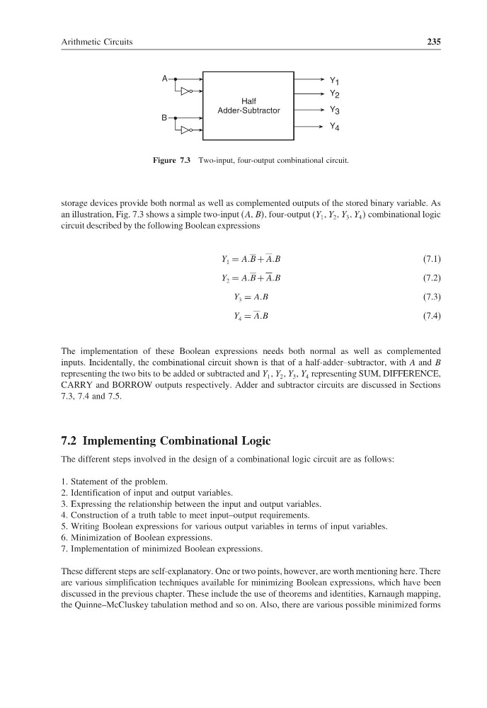
Figure 7.3 Two-input, four-output combinational circuit.
storage devices provide both normal as well as complemented outputs of the stored binary variable. As
an illustration, Fig. 7.3 shows a simple two-input (A, BB, four-output (Y 1 , Y 2 , Y 3 , Y 4 combinational logic
circuit described by the following Boolean expressions
Y 1 = AAB + AAB
(7.1)
Y 2 = AAB + AAB
(7.2)
Y 3 = AAB
(7.3)
Y 4 = AAB
(7.4)
The implementation of these Boolean expressions needs both normal as well as complemented
inputs. Incidentally, the combinational circuit shown is that of a half-adder–subtractor, with A and B
representing the two bits to be added or subtracted and Y 1 Y 2 , Y 3 , Y 4 representing SUM, DIFFERENCE,
CARRY and BORROW outputs respectively. Adder and subtractor circuits are discussed in Sections
7.3, 7.4 and 7.5.
7.2 Implementing Combinational Logic
The different steps involved in the design of a combinational logic circuit are as follows:
1. Statement of the problem.
2. Identification of input and output variables.
3. Expressing the relationship between the input and output variables.
4. Construction of a truth table to meet input–output requirements.
5. Writing Boolean expressions for various output variables in terms of input variables.
6. Minimization of Boolean expressions.
7. Implementation of minimized Boolean expressions.
These different steps are self-explanatory. One or two points, however, are worth mentioning here. There
are various simplification techniques available for minimizing Boolean expressions, which have been
discussed in the previous chapter. These include the use of theorems and identities, Karnaugh mapping,
the Quinne–McCluskey tabulation method and so on. Also, there are various possible minimized forms
235
Half
Adder-Subtractor
A
B
Y 1
Y 2
Y 3
Y 4
Figure 7.3 Two-input, four-output combinational circuit.
storage devices provide both normal as well as complemented outputs of the stored binary variable. As
an illustration, Fig. 7.3 shows a simple two-input (A, BB, four-output (Y 1 , Y 2 , Y 3 , Y 4 combinational logic
circuit described by the following Boolean expressions
Y 1 = AAB + AAB
(7.1)
Y 2 = AAB + AAB
(7.2)
Y 3 = AAB
(7.3)
Y 4 = AAB
(7.4)
The implementation of these Boolean expressions needs both normal as well as complemented
inputs. Incidentally, the combinational circuit shown is that of a half-adder–subtractor, with A and B
representing the two bits to be added or subtracted and Y 1 Y 2 , Y 3 , Y 4 representing SUM, DIFFERENCE,
CARRY and BORROW outputs respectively. Adder and subtractor circuits are discussed in Sections
7.3, 7.4 and 7.5.
7.2 Implementing Combinational Logic
The different steps involved in the design of a combinational logic circuit are as follows:
1. Statement of the problem.
2. Identification of input and output variables.
3. Expressing the relationship between the input and output variables.
4. Construction of a truth table to meet input–output requirements.
5. Writing Boolean expressions for various output variables in terms of input variables.
6. Minimization of Boolean expressions.
7. Implementation of minimized Boolean expressions.
These different steps are self-explanatory. One or two points, however, are worth mentioning here. There
are various simplification techniques available for minimizing Boolean expressions, which have been
discussed in the previous chapter. These include the use of theorems and identities, Karnaugh mapping,
the Quinne–McCluskey tabulation method and so on. Also, there are various possible minimized forms