

178
Digital Electronics
74S00
74S00
74S00
20
2
1
74S00
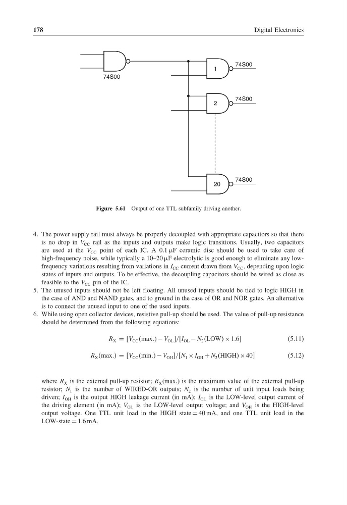
Figure 5.61 Output of one TTL subfamily driving another.
4. The power supply rail must always be properly decoupled with appropriate capacitors so that there
is no drop in V CC rail as the inputs and outputs make logic transitions. Usually, two capacitors
are used at the V CC point of each IC. A 0.1 F ceramic disc should be used to take care of
high-frequency noise, while typically a 10–20 F electrolytic is good enough to eliminate any lowfrequency variations resulting from variations in I CC current drawn from V CC , depending upon logic
states of inputs and outputs. To be effective, the decoupling capacitors should be wired as close as
feasible to the V CC pin of the IC.
5. The unused inputs should not be left floating. All unused inputs should be tied to logic HIGH in
the case of AND and NAND gates, and to ground in the case of OR and NOR gates. An alternative
is to connect the unused input to one of the used inputs.
6. While using open collector devices, resistive pull-up should be used. The value of pull-up resistance
should be determined from the following equations:
R X = V CC max − V OL //I OL − N 2 LOW × 16
(5.11)
R X max = V CC min − V OH //N 1 × I OH + N 2 HIGH × 40
(5.12)
where R X is the external pull-up resistor; R X (max.) is the maximum value of the external pull-up
resistor; N 1 is the number of WIRED-OR outputs; N 2 is the number of unit input loads being
driven; I OH is the output HIGH leakage current (in mA); I OL is the LOW-level output current of
the driving element (in mA); V OL is the LOW-level output voltage; and V OH is the HIGH-level
output voltage. One TTL unit load in the HIGH state = 40 mA, and one TTL unit load in the
LOW-state = 1.6 mA.
Digital Electronics
74S00
74S00
74S00
20
2
1
74S00
Figure 5.61 Output of one TTL subfamily driving another.
4. The power supply rail must always be properly decoupled with appropriate capacitors so that there
is no drop in V CC rail as the inputs and outputs make logic transitions. Usually, two capacitors
are used at the V CC point of each IC. A 0.1 F ceramic disc should be used to take care of
high-frequency noise, while typically a 10–20 F electrolytic is good enough to eliminate any lowfrequency variations resulting from variations in I CC current drawn from V CC , depending upon logic
states of inputs and outputs. To be effective, the decoupling capacitors should be wired as close as
feasible to the V CC pin of the IC.
5. The unused inputs should not be left floating. All unused inputs should be tied to logic HIGH in
the case of AND and NAND gates, and to ground in the case of OR and NOR gates. An alternative
is to connect the unused input to one of the used inputs.
6. While using open collector devices, resistive pull-up should be used. The value of pull-up resistance
should be determined from the following equations:
R X = V CC max − V OL //I OL − N 2 LOW × 16
(5.11)
R X max = V CC min − V OH //N 1 × I OH + N 2 HIGH × 40
(5.12)
where R X is the external pull-up resistor; R X (max.) is the maximum value of the external pull-up
resistor; N 1 is the number of WIRED-OR outputs; N 2 is the number of unit input loads being
driven; I OH is the output HIGH leakage current (in mA); I OL is the LOW-level output current of
the driving element (in mA); V OL is the LOW-level output voltage; and V OH is the HIGH-level
output voltage. One TTL unit load in the HIGH state = 40 mA, and one TTL unit load in the
LOW-state = 1.6 mA.