

Logic Families
177
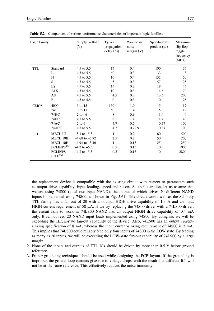
Table 5.2 Comparison of various performance characteristics of important logic families.
Logic family
Supply voltage
(V)
Typical
propagation
delay (ns)
Worst-case
noise
margin (V)
Speed–power
product (pJ)
Maximum
flip-flop
toggle
frequency
(MHz)
TTL
Standard
4.5 to 5.5
17
04
100
35
L
4.5 to 5.5
60
03
3 3
3
H
4.5 to 5.5
10
04
132
50
S
4.5 to 5.5
5
03
57
125
LS
4.5 to 5.5
15
03
1 8
4 5
ALS
4.5 to 5.5
10
03
4 8
7 0
AS
4.5 to 5.5
45
0 3
1 3 6
200
F
4.5 to 5.5
6
03
10
125
CMOS
4000
3 to 15
150
10
5
1 2
74C
3 to 13
50
14
5
1 2
74HC
2 to –6
8
09
1 4
4 0
74HCT
4.5 to 5.5
8
14
1 4
4 0
74AC
2 to 6
47
0 7
0 37
100
74ACT
4.5 to 5.5
47
0 729
0 37
100
ECL
MECL III
–5.1 to –5.3
1
02
60
500
MECL 10K
–4.68 to –5.72
25
0 2
50
200
MECL 10H
–4.94 to –5.46
1
015
25
250
ECLINPS
TM
–4.2 to –5.5
05
0 15
10
1000
ECLINPS
LITE
TM
–4.2 to –5.5
02
0 15
10
2800
the replacement device is compatible with the existing circuit with respect to parameters such
as output drive capability, input loading, speed and so on. As an illustration, let us assume that
we are using 74S00 (quad two-input NAND), the output of which drives 20 different NAND
inputs implemented using 74S00, as shown in Fig. 5.61. This circuit works well as the Schottky
TTL family has a fan-out of 20 with an output HIGH drive capability of 1 mA and an input
HIGH current requirement of 50 A. If we try replacing the 74S00 driver with a 74LS00 driver,
the circuit fails to work as 74LS00 NAND has an output HIGH drive capability of 0.4 mA
only. It cannot feed 20 NAND input loads implemented using 74S00. By doing so, we will be
exceeding the HIGH-state fan-out capability of the device. Also, 74LS00 has an output currentsinking specification of 8 mA, whereas the input current-sinking requirement of 74S00 is 2 mA.
This implies that 74LS00 could reliably feed only four inputs of 74S00 in the LOW state. By feeding
as many as 20 inputs, we will be exceeding the LOW-state fan-out capability of 74LS00 by a large
margin.
2. None of the inputs and outputs of TTL ICs should be driven by more than 0.5 V below ground
reference.
3. Proper grounding techniques should be used while designing the PCB layout. If the grounding is
improper, the ground loop currents give rise to voltage drops, with the result that different ICs will
not be at the same reference. This effectively reduces the noise immunity.
177
Table 5.2 Comparison of various performance characteristics of important logic families.
Logic family
Supply voltage
(V)
Typical
propagation
delay (ns)
Worst-case
noise
margin (V)
Speed–power
product (pJ)
Maximum
flip-flop
toggle
frequency
(MHz)
TTL
Standard
4.5 to 5.5
17
04
100
35
L
4.5 to 5.5
60
03
3 3
3
H
4.5 to 5.5
10
04
132
50
S
4.5 to 5.5
5
03
57
125
LS
4.5 to 5.5
15
03
1 8
4 5
ALS
4.5 to 5.5
10
03
4 8
7 0
AS
4.5 to 5.5
45
0 3
1 3 6
200
F
4.5 to 5.5
6
03
10
125
CMOS
4000
3 to 15
150
10
5
1 2
74C
3 to 13
50
14
5
1 2
74HC
2 to –6
8
09
1 4
4 0
74HCT
4.5 to 5.5
8
14
1 4
4 0
74AC
2 to 6
47
0 7
0 37
100
74ACT
4.5 to 5.5
47
0 729
0 37
100
ECL
MECL III
–5.1 to –5.3
1
02
60
500
MECL 10K
–4.68 to –5.72
25
0 2
50
200
MECL 10H
–4.94 to –5.46
1
015
25
250
ECLINPS
TM
–4.2 to –5.5
05
0 15
10
1000
ECLINPS
LITE
TM
–4.2 to –5.5
02
0 15
10
2800
the replacement device is compatible with the existing circuit with respect to parameters such
as output drive capability, input loading, speed and so on. As an illustration, let us assume that
we are using 74S00 (quad two-input NAND), the output of which drives 20 different NAND
inputs implemented using 74S00, as shown in Fig. 5.61. This circuit works well as the Schottky
TTL family has a fan-out of 20 with an output HIGH drive capability of 1 mA and an input
HIGH current requirement of 50 A. If we try replacing the 74S00 driver with a 74LS00 driver,
the circuit fails to work as 74LS00 NAND has an output HIGH drive capability of 0.4 mA
only. It cannot feed 20 NAND input loads implemented using 74S00. By doing so, we will be
exceeding the HIGH-state fan-out capability of the device. Also, 74LS00 has an output currentsinking specification of 8 mA, whereas the input current-sinking requirement of 74S00 is 2 mA.
This implies that 74LS00 could reliably feed only four inputs of 74S00 in the LOW state. By feeding
as many as 20 inputs, we will be exceeding the LOW-state fan-out capability of 74LS00 by a large
margin.
2. None of the inputs and outputs of TTL ICs should be driven by more than 0.5 V below ground
reference.
3. Proper grounding techniques should be used while designing the PCB layout. If the grounding is
improper, the ground loop currents give rise to voltage drops, with the result that different ICs will
not be at the same reference. This effectively reduces the noise immunity.