

172
Digital Electronics
Q 1
Q 3
Q 4
Q 5
Q 6
Q 2
Q 9
Q8
+V DD
A
B
Q 7
Y=A.B
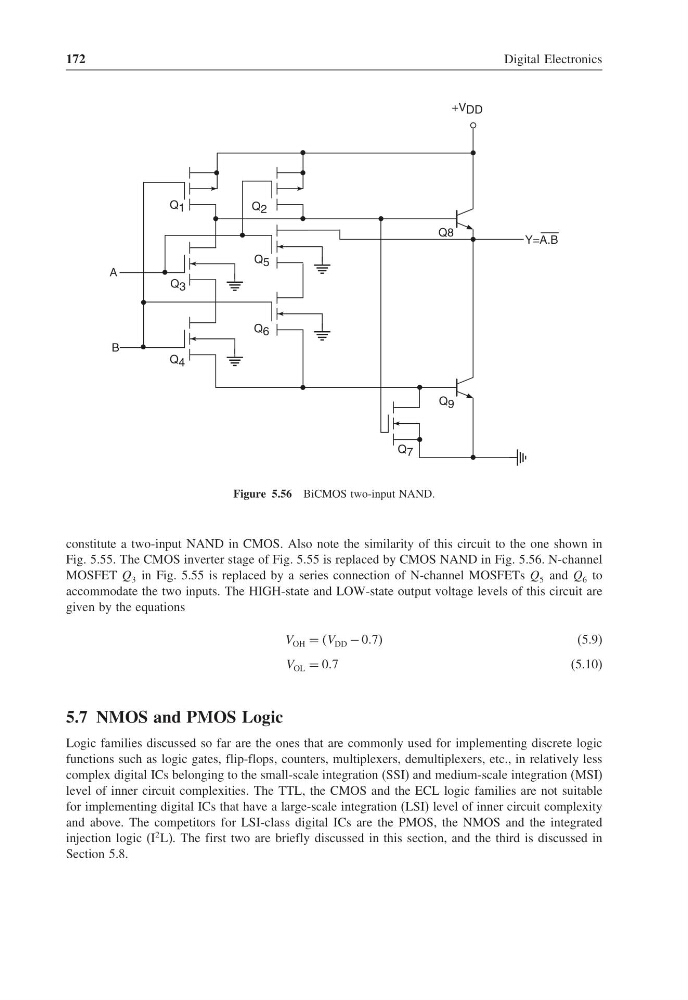
Figure 5.56 BiCMOS two-input NAND.
constitute a two-input NAND in CMOS. Also note the similarity of this circuit to the one shown in
Fig. 5.55. The CMOS inverter stage of Fig. 5.55 is replaced by CMOS NAND in Fig. 5.56. N-channel
MOSFET Q 3 in Fig. 5.55 is replaced by a series connection of N-channel MOSFETs Q 5 and Q 6 to
accommodate the two inputs. The HIGH-state and LOW-state output voltage levels of this circuit are
given by the equations
V OH = V DD − 07
(5.9)
V OL = 07
(5.10)
5.7 NMOS and PMOS Logic
Logic families discussed so far are the ones that are commonly used for implementing discrete logic
functions such as logic gates, flip-flops, counters, multiplexers, demultiplexers, etc., in relatively less
complex digital ICs belonging to the small-scale integration (SSI) and medium-scale integration (MSI)
level of inner circuit complexities. The TTL, the CMOS and the ECL logic families are not suitable
for implementing digital ICs that have a large-scale integration (LSI) level of inner circuit complexity
and above. The competitors for LSI-class digital ICs are the PMOS, the NMOS and the integrated
injection logic (I
2 L). The first two are briefly discussed in this section, and the third is discussed in
Section 5.8.
Digital Electronics
Q 1
Q 3
Q 4
Q 5
Q 6
Q 2
Q 9
Q8
+V DD
A
B
Q 7
Y=A.B
Figure 5.56 BiCMOS two-input NAND.
constitute a two-input NAND in CMOS. Also note the similarity of this circuit to the one shown in
Fig. 5.55. The CMOS inverter stage of Fig. 5.55 is replaced by CMOS NAND in Fig. 5.56. N-channel
MOSFET Q 3 in Fig. 5.55 is replaced by a series connection of N-channel MOSFETs Q 5 and Q 6 to
accommodate the two inputs. The HIGH-state and LOW-state output voltage levels of this circuit are
given by the equations
V OH = V DD − 07
(5.9)
V OL = 07
(5.10)
5.7 NMOS and PMOS Logic
Logic families discussed so far are the ones that are commonly used for implementing discrete logic
functions such as logic gates, flip-flops, counters, multiplexers, demultiplexers, etc., in relatively less
complex digital ICs belonging to the small-scale integration (SSI) and medium-scale integration (MSI)
level of inner circuit complexities. The TTL, the CMOS and the ECL logic families are not suitable
for implementing digital ICs that have a large-scale integration (LSI) level of inner circuit complexity
and above. The competitors for LSI-class digital ICs are the PMOS, the NMOS and the integrated
injection logic (I
2 L). The first two are briefly discussed in this section, and the third is discussed in
Section 5.8.