

Logic Families
171
category, the bipolar component is optimized to produce high-performance circuitry. In the following
paragraphs, we will briefly describe the basic BiCMOS inverter and NAND circuits.
5.6.1 BiCMOS Inverter
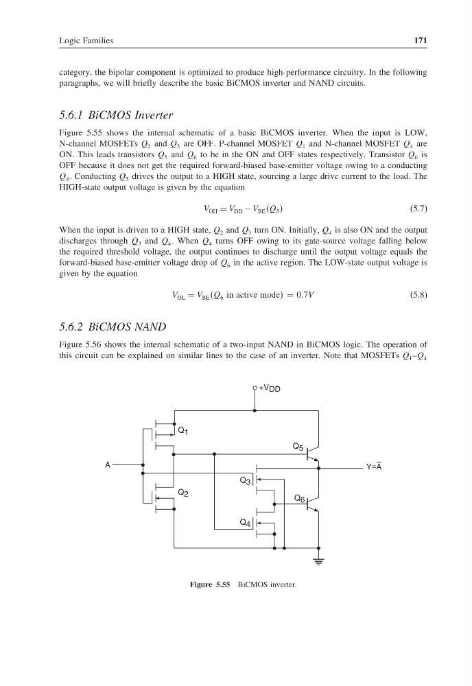
Figure 5.55 shows the internal schematic of a basic BiCMOS inverter. When the input is LOW,
N-channel MOSFETs Q 2 and Q 3 are OFF. P-channel MOSFET Q 1 and N-channel MOSFET Q 4 are
ON. This leads transistors Q 5 and Q 6 to be in the ON and OFF states respectively. Transistor Q 6 is
OFF because it does not get the required forward-biased base-emitter voltage owing to a conducting
Q 4 . Conducting Q 5 drives the output to a HIGH state, sourcing a large drive current to the load. The
HIGH-state output voltage is given by the equation
V OH = V DD − V BE Q 5
(5.7)
When the input is driven to a HIGH state, Q 2 and Q 3 turn ON. Initially, Q 4 is also ON and the output
discharges through Q 3 and Q 4 . When Q 4 turns OFF owing to its gate-source voltage falling below
the required threshold voltage, the output continues to discharge until the output voltage equals the
forward-biased base-emitter voltage drop of Q 6 in the active region. The LOW-state output voltage is
given by the equation
V OL = V BE Q 6 in active mode = 07V
(5.8)
5.6.2 BiCMOS NAND
Figure 5.56 shows the internal schematic of a two-input NAND in BiCMOS logic. The operation of
this circuit can be explained on similar lines to the case of an inverter. Note that MOSFETs Q 1 –Q 4
Q 1
+V DD
A
Q 5
Q 6
Y=A
Q 3
Q 4
Q 2
Figure 5.55 BiCMOS inverter.
171
category, the bipolar component is optimized to produce high-performance circuitry. In the following
paragraphs, we will briefly describe the basic BiCMOS inverter and NAND circuits.
5.6.1 BiCMOS Inverter
Figure 5.55 shows the internal schematic of a basic BiCMOS inverter. When the input is LOW,
N-channel MOSFETs Q 2 and Q 3 are OFF. P-channel MOSFET Q 1 and N-channel MOSFET Q 4 are
ON. This leads transistors Q 5 and Q 6 to be in the ON and OFF states respectively. Transistor Q 6 is
OFF because it does not get the required forward-biased base-emitter voltage owing to a conducting
Q 4 . Conducting Q 5 drives the output to a HIGH state, sourcing a large drive current to the load. The
HIGH-state output voltage is given by the equation
V OH = V DD − V BE Q 5
(5.7)
When the input is driven to a HIGH state, Q 2 and Q 3 turn ON. Initially, Q 4 is also ON and the output
discharges through Q 3 and Q 4 . When Q 4 turns OFF owing to its gate-source voltage falling below
the required threshold voltage, the output continues to discharge until the output voltage equals the
forward-biased base-emitter voltage drop of Q 6 in the active region. The LOW-state output voltage is
given by the equation
V OL = V BE Q 6 in active mode = 07V
(5.8)
5.6.2 BiCMOS NAND
Figure 5.56 shows the internal schematic of a two-input NAND in BiCMOS logic. The operation of
this circuit can be explained on similar lines to the case of an inverter. Note that MOSFETs Q 1 –Q 4
Q 1
+V DD
A
Q 5
Q 6
Y=A
Q 3
Q 4
Q 2
Figure 5.55 BiCMOS inverter.