

160
Digital Electronics
Y=(A+B).(C+D)
D
B
C
A
+V DD
Q 7
Q 8
Q 5
Q 6
Q 3
Q 4
Q 1
Q 2
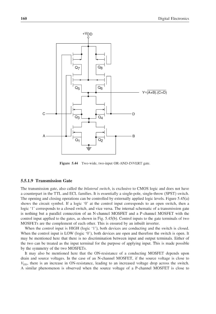
Figure 5.44 Two-wide, two-input OR-AND-INVERT gate.
5.5.1.9 Transmission Gate
The transmission gate, also called the bilateral switch, is exclusive to CMOS logic and does not have
a counterpart in the TTL and ECL families. It is essentially a single-pole, single-throw (SPST) switch.
The opening and closing operations can be controlled by externally applied logic levels. Figure 5.45(a)
shows the circuit symbol. If a logic ‘0’ at the control input corresponds to an open switch, then a
logic ‘1’ corresponds to a closed switch, and vice versa. The internal schematic of a transmission gate
is nothing but a parallel connection of an N-channel MOSFET and a P-channel MOSFET with the
control input applied to the gates, as shown in Fig. 5.45(b). Control inputs to the gate terminals of two
MOSFETs are the complement of each other. This is ensured by an inbuilt inverter.
When the control input is HIGH (logic ‘1’), both devices are conducting and the switch is closed.
When the control input is LOW (logic ‘0’), both devices are open and therefore the switch is open. It
may be mentioned here that there is no discrimination between input and output terminals. Either of
the two can be treated as the input terminal for the purpose of applying input. This is made possible
by the symmetry of the two MOSFETs.
It may also be mentioned here that the ON-resistance of a conducting MOSFET depends upon
drain and source voltages. In the case of an N-channel MOSFET, if the source voltage is close to
V DD , there is an increase in ON-resistance, leading to an increased voltage drop across the switch.
A similar phenomenon is observed when the source voltage of a P-channel MOSFET is close to
Digital Electronics
Y=(A+B).(C+D)
D
B
C
A
+V DD
Q 7
Q 8
Q 5
Q 6
Q 3
Q 4
Q 1
Q 2
Figure 5.44 Two-wide, two-input OR-AND-INVERT gate.
5.5.1.9 Transmission Gate
The transmission gate, also called the bilateral switch, is exclusive to CMOS logic and does not have
a counterpart in the TTL and ECL families. It is essentially a single-pole, single-throw (SPST) switch.
The opening and closing operations can be controlled by externally applied logic levels. Figure 5.45(a)
shows the circuit symbol. If a logic ‘0’ at the control input corresponds to an open switch, then a
logic ‘1’ corresponds to a closed switch, and vice versa. The internal schematic of a transmission gate
is nothing but a parallel connection of an N-channel MOSFET and a P-channel MOSFET with the
control input applied to the gates, as shown in Fig. 5.45(b). Control inputs to the gate terminals of two
MOSFETs are the complement of each other. This is ensured by an inbuilt inverter.
When the control input is HIGH (logic ‘1’), both devices are conducting and the switch is closed.
When the control input is LOW (logic ‘0’), both devices are open and therefore the switch is open. It
may be mentioned here that there is no discrimination between input and output terminals. Either of
the two can be treated as the input terminal for the purpose of applying input. This is made possible
by the symmetry of the two MOSFETs.
It may also be mentioned here that the ON-resistance of a conducting MOSFET depends upon
drain and source voltages. In the case of an N-channel MOSFET, if the source voltage is close to
V DD , there is an increase in ON-resistance, leading to an increased voltage drop across the switch.
A similar phenomenon is observed when the source voltage of a P-channel MOSFET is close to