

Logic Families
161
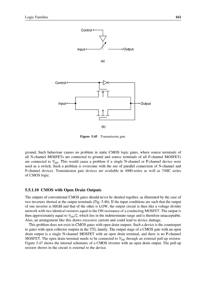
Figure 5.45 Transmission gate.
ground. Such behaviour causes no problem in static CMOS logic gates, where source terminals of
all N-channel MOSFETs are connected to ground and source terminals of all P-channel MOSFETs
are connected to V DD . This would cause a problem if a single N-channel or P-channel device were
used as a switch. Such a problem is overcome with the use of parallel connection of N-channel and
P-channel devices. Transmission gate devices are available in 4000-series as well as 74HC series
of CMOS logic.
5.5.1.10 CMOS with Open Drain Outputs
The outputs of conventional CMOS gates should never be shorted together, as illustrated by the case of
two inverters shorted at the output terminals (Fig. 5.46). If the input conditions are such that the output
of one inverter is HIGH and that of the other is LOW, the output circuit is then like a voltage divider
network with two identical resistors equal to the ON-resistance of a conducting MOSFET. The output is
then approximately equal to V DD /2, which lies in the indeterminate range and is therefore unacceptable.
Also, an arrangement like this draws excessive current and could lead to device damage.
This problem does not exist in CMOS gates with open drain outputs. Such a device is the counterpart
to gates with open collector outputs in the TTL family. The output stage of a CMOS gate with an open
drain output is a single N-channel MOSFET with an open drain terminal, and there is no P-channel
MOSFET. The open drain terminal needs to be connected to V DD through an external pull-up resistor.
Figure 5.47 shows the internal schematic of a CMOS inverter with an open drain output. The pull-up
resistor shown in the circuit is external to the device.
161
Figure 5.45 Transmission gate.
ground. Such behaviour causes no problem in static CMOS logic gates, where source terminals of
all N-channel MOSFETs are connected to ground and source terminals of all P-channel MOSFETs
are connected to V DD . This would cause a problem if a single N-channel or P-channel device were
used as a switch. Such a problem is overcome with the use of parallel connection of N-channel and
P-channel devices. Transmission gate devices are available in 4000-series as well as 74HC series
of CMOS logic.
5.5.1.10 CMOS with Open Drain Outputs
The outputs of conventional CMOS gates should never be shorted together, as illustrated by the case of
two inverters shorted at the output terminals (Fig. 5.46). If the input conditions are such that the output
of one inverter is HIGH and that of the other is LOW, the output circuit is then like a voltage divider
network with two identical resistors equal to the ON-resistance of a conducting MOSFET. The output is
then approximately equal to V DD /2, which lies in the indeterminate range and is therefore unacceptable.
Also, an arrangement like this draws excessive current and could lead to device damage.
This problem does not exist in CMOS gates with open drain outputs. Such a device is the counterpart
to gates with open collector outputs in the TTL family. The output stage of a CMOS gate with an open
drain output is a single N-channel MOSFET with an open drain terminal, and there is no P-channel
MOSFET. The open drain terminal needs to be connected to V DD through an external pull-up resistor.
Figure 5.47 shows the internal schematic of a CMOS inverter with an open drain output. The pull-up
resistor shown in the circuit is external to the device.